Home > Press > Columbia Researchers Squeeze Light into Nanoscale Devices and Circuits: Team is first to directly image propagation and dynamics of graphene plasmons at very low temperatures; findings could impact optical communications and signal processing
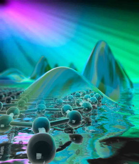 |
| The best pictorial representation of a surface plasmon polariton is in terms of a �ripple� of electron density on the surface of graphene sample. Dmitri Basov/Columbia University |
Abstract:
As electronic devices and circuits shrink into the nanoscale, the ability to transfer data on a chip, at low power with little energy loss, is becoming a critical challenge. Over the past decade, squeezing light into tiny devices and circuits has been a major goal of nanophotonics researchers. Electronic oscillations at the surface of metals, known as surface plasmon polaritons or plasmons for short, have become an intense area of focus. Plasmons are hybrids of light (photons) and electrons in a metal. If researchers can harness this nanolight, they will be able to improve sensing, subwavelength waveguiding, and optical transmission of signals.
Columbia Researchers Squeeze Light into Nanoscale Devices and Circuits: Team is first to directly image propagation and dynamics of graphene plasmons at very low temperatures; findings could impact optical communications and signal processing
New York, NY | Posted on May 23rd, 2018Columbia investigators have made a major breakthrough in this research, with their invention of a novel �home-built� cryogenic near-field optical microscope that has enabled them to directly image, for the first time, the propagation and dynamics of graphene plasmons at variable temperatures down to negative 250 degrees Celsius. The study was published online today in Nature.
�Our temperature-dependent study now gives us direct physical insight into the fundamental physics of plasmon propagation in graphene,� says Dimitri N. Basov, professor of physics at Columbia University, who led the study together with colleagues Cory Dean (physics) and James Hone (mechanical engineering, Columbia Engineering). �This insight was impossible to attain in previous nanoimaging studies done at room temperature. We were particularly surprised at discovering, after many years of failed attempts to get anywhere close, that compact nanolight can travel along the surface of graphene for distances of many tens of microns without unwanted scattering. The physics limiting the travel range of nanolight is a fundamental finding of our study and may lead to new applications in sensors, imaging, and signal processing.�
Basov, Dean, and Hone bring together years of experience in working with graphene, the one-atom-thick material that is one of the most promising candidates for novel photonic materials. Graphene�s optical properties are readily tunable and can be altered at ultrafast time scales. However, implementing nanolight without introducing unwanted dissipation in graphene has been very difficult to achieve.
The Columbia researchers developed a practical approach to confining light to the nanoscale. They knew they could form plasmon-polaritons, or resonant modes, in the graphene that propagate through the material as hybrid excitations of light and mobile electrons. These plasmon-polariton modes can confine the energy of electromagnetic radiation, or light, down to the nanoscale. The challenge was how to visualize these waves with ultra-high spatial resolution, so that they could study the performance of plasmonic modes at varying temperatures.
Alexander S. McLeod, a postdoctoral research scientist in the Basov Nano-optics Laboratory, built a unique microscope that enabled the team to explore the plasmon-polariton waves at high resolution while they cooled the graphene to cryogenic temperatures. Lowering the temperatures allowed them to �turn off� various scattering, or dissipation, mechanisms, one after another, as they cooled down their samples and learned which mechanisms were relevant.
�Now that our novel nanoimaging capabilities are deployed to low temperatures, we can see directly the unmitigated wave propagation of collective light-and-charge excitations within graphene,� says McLeod, co-lead author of the study with Guangxin Ni, also a postdoctoral research scientist in Basov�s lab. �Often times in physics, as in life, seeing truly is believing! The record-breaking travel range of these waves shows they�re destined to take on a life of their own, funneling signals and information back and forth inside next-generation optical devices.�
The study is the first to demonstrate the fundamental limitations for the propagation of plasmon polariton waves in graphene. The team found that graphene plasmons propagate ballistically, across tens of micrometers, throughout the tiny device. These plasmon modes are confined within a volume of space hundreds, if not thousands, of times smaller than that occupied by freely propagating light.
Plasmons in graphene can be tuned and controlled via an external electric field, which gives graphene a big advantage over conventional plasmonic media such as metal surfaces, which are inherently non-tunable. Moreover, the lifetimes of plasmon waves in graphene are now found to exceed those in metals by a factor of 10 to a 100, while propagating over comparably longer distances. These features offer enormous advantages for graphene as a plasmonic medium in next-generation opto-electronic circuits.
�Our results establish that graphene ranks among the best candidate materials for infrared plasmonics, with applications in imaging, sensing, and nano-scale manipulation of light,� says Hone. �Furthermore, our findings reveal the fundamental physics of processes that limit propagation of plasmon waves in graphene. This monumental insight will guide future efforts in nanostructure engineering, which may be able to remove the remaining roadblocks for long-range travel of versatile nanoconfined light within future optical devices.�
The current study is the beginning of a series of low-temperature investigations focused on controlling and manipulating confined plasmons in nanoscale optoelectronic graphene devices. The team is now using low-temperature nanoimaging to explore novel plasmonics effects such as electrically-induced plasmonic reflection and modulation, topological chiral plasmons, and also superconducting plasmonics in the very recently discovered �magic angle� system of twisted bilayer graphene.
####
About Columbia University School of Engineering and Applied Science
Columbia Engineering, based in New York City, is one of the top engineering schools in the U.S. and one of the oldest in the nation. Also known as The Fu Foundation School of Engineering and Applied Science, the School expands knowledge and advances technology through the pioneering research of its more than 200 faculty, while educating undergraduate and graduate students in a collaborative environment to become leaders informed by a firm foundation in engineering. The School�s faculty are at the center of the University�s cross-disciplinary research, contributing to the Data Science Institute, Earth Institute, Zuckerman Mind Brain Behavior Institute, Precision Medicine Initiative, and the Columbia Nano Initiative. Guided by its strategic vision, �Columbia Engineering for Humanity,� the School aims to translate ideas into innovations that foster a sustainable, healthy, secure, connected, and creative humanity.Columbia Engineering, based in New York City, is one of the top engineering schools in the U.S. and one of the oldest in the nation. Also known as The Fu Foundation School of Engineering and Applied Science, the School expands knowledge and advances technology through the pioneering research of its more than 200 faculty, while educating undergraduate and graduate students in a collaborative environment to become leaders informed by a firm foundation in engineering. The School�s faculty are at the center of the University�s cross-disciplinary research, contributing to the Data Science Institute, Earth Institute, Zuckerman Mind Brain Behavior Institute, Precision Medicine Initiative, and the Columbia Nano Initiative. Guided by its strategic vision, �Columbia Engineering for Humanity,� the School aims to translate ideas into innovations that foster a sustainable, healthy, secure, connected, and creative humanity.
For more information, please click here
Contacts:
Holly Evarts
Director of Strategic Communications and Media Relations
212-854-3206 (o)
347-453-7408 (c)
Copyright © Columbia University School of Engineering and Applied Science
If you have a comment, please Contact us.Issuers of news releases, not 7th Wave, Inc. or Nanotechnology Now, are solely responsible for the accuracy of the content.
Bookmark:


| Related Links |
| Related News Press |
News and information
![]() Quantum computer improves AI predictions April 17th, 2026
Quantum computer improves AI predictions April 17th, 2026
![]() Flexible sensor gains sensitivity under pressure April 17th, 2026
Flexible sensor gains sensitivity under pressure April 17th, 2026
![]() A reusable chip for particulate matter sensing April 17th, 2026
A reusable chip for particulate matter sensing April 17th, 2026
![]() Detecting vibrational quantum beating in the predissociation dynamics of SF6 using time-resolved photoelectron spectroscopy April 17th, 2026
Detecting vibrational quantum beating in the predissociation dynamics of SF6 using time-resolved photoelectron spectroscopy April 17th, 2026
Imaging
![]() Simple algorithm paired with standard imaging tool could predict failure in lithium metal batteries August 8th, 2025
Simple algorithm paired with standard imaging tool could predict failure in lithium metal batteries August 8th, 2025
Graphene/ Graphite
![]() Electrifying results shed light on graphene foam as a potential material for lab grown cartilage June 6th, 2025
Electrifying results shed light on graphene foam as a potential material for lab grown cartilage June 6th, 2025
![]() Breakthrough in proton barrier films using pore-free graphene oxide: Kumamoto University researchers achieve new milestone in advanced coating technologies September 13th, 2024
Breakthrough in proton barrier films using pore-free graphene oxide: Kumamoto University researchers achieve new milestone in advanced coating technologies September 13th, 2024
![]() NRL discovers two-dimensional waveguides February 16th, 2024
NRL discovers two-dimensional waveguides February 16th, 2024
Plasmonics
![]() Unveiling the power of hot carriers in plasmonic nanostructures August 16th, 2024
Unveiling the power of hot carriers in plasmonic nanostructures August 16th, 2024
Govt.-Legislation/Regulation/Funding/Policy
![]() Quantum computer improves AI predictions April 17th, 2026
Quantum computer improves AI predictions April 17th, 2026
![]() Metasurfaces smooth light to boost magnetic sensing precision January 30th, 2026
Metasurfaces smooth light to boost magnetic sensing precision January 30th, 2026
![]() New imaging approach transforms study of bacterial biofilms August 8th, 2025
New imaging approach transforms study of bacterial biofilms August 8th, 2025
Possible Futures
![]() A fundamentally new therapeutic approach to cystic fibrosis: Nanobody repairs cellular defect April 17th, 2026
A fundamentally new therapeutic approach to cystic fibrosis: Nanobody repairs cellular defect April 17th, 2026
![]() UC Irvine physicists discover method to reverse �quantum scrambling� : The work addresses the problem of information loss in quantum computing system April 17th, 2026
UC Irvine physicists discover method to reverse �quantum scrambling� : The work addresses the problem of information loss in quantum computing system April 17th, 2026
Chip Technology
![]() A reusable chip for particulate matter sensing April 17th, 2026
A reusable chip for particulate matter sensing April 17th, 2026
![]() Metasurfaces smooth light to boost magnetic sensing precision January 30th, 2026
Metasurfaces smooth light to boost magnetic sensing precision January 30th, 2026
Optical computing/Photonic computing
![]() ICFO researchers overcome long-standing bottleneck in single photon detection with twisted 2D materials August 8th, 2025
ICFO researchers overcome long-standing bottleneck in single photon detection with twisted 2D materials August 8th, 2025
![]() Programmable electron-induced color router array May 14th, 2025
Programmable electron-induced color router array May 14th, 2025
Nanoelectronics
![]() Lab to industry: InSe wafer-scale breakthrough for future electronics August 8th, 2025
Lab to industry: InSe wafer-scale breakthrough for future electronics August 8th, 2025
![]() Interdisciplinary: Rice team tackles the future of semiconductors Multiferroics could be the key to ultralow-energy computing October 6th, 2023
Interdisciplinary: Rice team tackles the future of semiconductors Multiferroics could be the key to ultralow-energy computing October 6th, 2023
![]() Key element for a scalable quantum computer: Physicists from Forschungszentrum J�lich and RWTH Aachen University demonstrate electron transport on a quantum chip September 23rd, 2022
Key element for a scalable quantum computer: Physicists from Forschungszentrum J�lich and RWTH Aachen University demonstrate electron transport on a quantum chip September 23rd, 2022
![]() Reduced power consumption in semiconductor devices September 23rd, 2022
Reduced power consumption in semiconductor devices September 23rd, 2022
Discoveries
![]() Quantum computer improves AI predictions April 17th, 2026
Quantum computer improves AI predictions April 17th, 2026
![]() Flexible sensor gains sensitivity under pressure April 17th, 2026
Flexible sensor gains sensitivity under pressure April 17th, 2026
![]() A reusable chip for particulate matter sensing April 17th, 2026
A reusable chip for particulate matter sensing April 17th, 2026
![]() Detecting vibrational quantum beating in the predissociation dynamics of SF6 using time-resolved photoelectron spectroscopy April 17th, 2026
Detecting vibrational quantum beating in the predissociation dynamics of SF6 using time-resolved photoelectron spectroscopy April 17th, 2026
Announcements
![]() A fundamentally new therapeutic approach to cystic fibrosis: Nanobody repairs cellular defect April 17th, 2026
A fundamentally new therapeutic approach to cystic fibrosis: Nanobody repairs cellular defect April 17th, 2026
![]() UC Irvine physicists discover method to reverse �quantum scrambling� : The work addresses the problem of information loss in quantum computing system April 17th, 2026
UC Irvine physicists discover method to reverse �quantum scrambling� : The work addresses the problem of information loss in quantum computing system April 17th, 2026
Interviews/Book Reviews/Essays/Reports/Podcasts/Journals/White papers/Posters
![]() A fundamentally new therapeutic approach to cystic fibrosis: Nanobody repairs cellular defect April 17th, 2026
A fundamentally new therapeutic approach to cystic fibrosis: Nanobody repairs cellular defect April 17th, 2026
![]() UC Irvine physicists discover method to reverse �quantum scrambling� : The work addresses the problem of information loss in quantum computing system April 17th, 2026
UC Irvine physicists discover method to reverse �quantum scrambling� : The work addresses the problem of information loss in quantum computing system April 17th, 2026
Tools
![]() Metasurfaces smooth light to boost magnetic sensing precision January 30th, 2026
Metasurfaces smooth light to boost magnetic sensing precision January 30th, 2026
![]() From sensors to smart systems: the rise of AI-driven photonic noses January 30th, 2026
From sensors to smart systems: the rise of AI-driven photonic noses January 30th, 2026
![]() Japan launches fully domestically produced quantum computer: Expo visitors to experience quantum computing firsthand August 8th, 2025
Japan launches fully domestically produced quantum computer: Expo visitors to experience quantum computing firsthand August 8th, 2025
Military
![]() Quantum engineers �squeeze� laser frequency combs to make more sensitive gas sensors January 17th, 2025
Quantum engineers �squeeze� laser frequency combs to make more sensitive gas sensors January 17th, 2025
![]() Chainmail-like material could be the future of armor: First 2D mechanically interlocked polymer exhibits exceptional flexibility and strength January 17th, 2025
Chainmail-like material could be the future of armor: First 2D mechanically interlocked polymer exhibits exceptional flexibility and strength January 17th, 2025
![]() Single atoms show their true color July 5th, 2024
Single atoms show their true color July 5th, 2024
![]() NRL charters Navy�s quantum inertial navigation path to reduce drift April 5th, 2024
NRL charters Navy�s quantum inertial navigation path to reduce drift April 5th, 2024
Grants/Sponsored Research/Awards/Scholarships/Gifts/Contests/Honors/Records
![]() Quantum computer improves AI predictions April 17th, 2026
Quantum computer improves AI predictions April 17th, 2026
![]() Detecting vibrational quantum beating in the predissociation dynamics of SF6 using time-resolved photoelectron spectroscopy April 17th, 2026
Detecting vibrational quantum beating in the predissociation dynamics of SF6 using time-resolved photoelectron spectroscopy April 17th, 2026
![]() Metasurfaces smooth light to boost magnetic sensing precision January 30th, 2026
Metasurfaces smooth light to boost magnetic sensing precision January 30th, 2026
Photonics/Optics/Lasers
![]() Metasurfaces smooth light to boost magnetic sensing precision January 30th, 2026
Metasurfaces smooth light to boost magnetic sensing precision January 30th, 2026
![]() From sensors to smart systems: the rise of AI-driven photonic noses January 30th, 2026
From sensors to smart systems: the rise of AI-driven photonic noses January 30th, 2026
|
|
||
|
|
||
| The latest news from around the world, FREE | ||
|
|
||
|
|
||
| Premium Products | ||
|
|
||
|
Only the news you want to read!
Learn More |
||
|
|
||
|
Full-service, expert consulting
Learn More |
||
|
|
||