Home > Press > Band Gaps, Made to Order: Engineers create atomically thin superlattice materials with precision
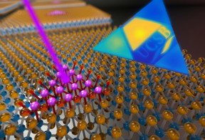 |
| This artist’s representation shows an electron beam (in purple) being used to create a 2D superlattice made up of quantum dots having extraordinary atomic-scale precision and placement. Photo Credit: PETER ALLEN |
Abstract:
Control is a constant challenge for materials scientists, who are always seeking the perfect material — and the perfect way of treating it — to induce exactly the right electronic or optical activity required for a given application.
Band Gaps, Made to Order: Engineers create atomically thin superlattice materials with precision
Santa Barbara, CA | Posted on September 26th, 2017One key challenge to modulating activity in a semiconductor is controlling its band gap. When a material is excited with energy, say, a light pulse, the wider its band gap, the shorter the wavelength of the light it emits. The narrower the band gap, the longer the wavelength.
As electronics and the devices that incorporate them — smartphones, laptops and the like — have become smaller and smaller, the semiconductor transistors that power them have shrunk to the point of being not much larger than an atom. They can’t get much smaller. To overcome this limitation, researchers are seeking ways to harness the unique characteristics of nanoscale atomic cluster arrays — known as quantum dot superlattices — for building next generation electronics such as large-scale quantum information systems. In the quantum realm, precision is even more important.
New research conducted by UC Santa Barbara’s Department of Electrical and Computer Engineering reveals a major advance in precision superlattices materials. The findings by Professor Kaustav Banerjee, his Ph.D. students Xuejun Xie, Jiahao Kang and Wei Cao, postdoctoral fellow Jae Hwan Chu and collaborators at Rice University appear in the journal Nature Scientific Reports.
Their team’s research uses a focused electron beam to fabricate a large-scale quantum dot superlattice on which each quantum dot has a specific pre-determined size positioned at a precise location on an atomically thin sheet of two-dimensional (2-D) semiconductor molybdenum disulphide (MoS2). When the focused electron beam interacts with the MoS2 monolayer, it turns that area — which is on the order of a nanometer in diameter — from semiconducting to metallic. The quantum dots can be placed less than four nanometers apart, so that they become an artificial crystal — essentially a new 2-D material where the band gap can be specified to order, from 1.8 to 1.4 electron volts (eV).
This is the first time that scientists have created a large-area 2-D superlattice — nanoscale atomic clusters in an ordered grid — on an atomically thin material on which both the size and location of quantum dots are precisely controlled. The process not only creates several quantum dots, but can also be applied directly to large-scale fabrication of 2-D quantum dot superlattices. “We can, therefore, change the overall properties of the 2-D crystal,” Banerjee said.
Each quantum dot acts as a quantum well, where electron-hole activity occurs, and all of the dots in the grid are close enough to each other to ensure interactions. The researchers can vary the spacing and size of the dots to vary the band gap, which determines the wavelength of light it emits.
“Using this technique, we can engineer the band gap to match the application,” Banerjee said. Quantum dot superlattices have been widely investigated for creating materials with tunable band gaps but all were made using “bottom-up” methods in which atoms naturally and spontaneously combine to form a macro-object. But those methods make it inherently difficult to design the lattice structure as desired and, thus, to achieve optimal performance.
As an example, depending on conditions, combining carbon atoms yields only two results in the bulk (or 3-D) form: graphite or diamond. These cannot be ‘tuned’ and so cannot make anything in between. But when atoms can be precisely positioned, the material can be designed with desired characteristics.
“Our approach overcomes the problems of randomness and proximity, enabling control of the band gap and all the other characteristics you might want the material to have — with a high level of precision,” Xie said. “This is a new way to make materials, and it will have many uses, particularly in quantum computing and communication applications. The dots on the superlattice are so close to each other that the electrons are coupled, an important requirement for quantum computing.”
The quantum dot is theoretically an artificial “atom.” The developed technique makes such design and “tuning” possible by enabling top-down control of the size and the position of the artificial atoms at large scale.
To demonstrate the level of control achieved, the authors produced an image of “UCSB” spelled out in a grid of quantum dots. By using different doses from the electron beam, they were able to cause different areas of the university’s initials to light up at different wavelengths.
“When you change the dose of the electron beam, you can change the size of the quantum dot in the local region, and once you do that, you can control the band gap of the 2-D material,” Banerjee explained. “If you say you want a band gap of 1.6 eV, I can give it to you. If you want 1.5 eV, I can do that, too, starting with the same material.”
This demonstration of tunable direct band gap could usher a new generation of light-emitting devices for photonics applications.
####
For more information, please click here
Contacts:
James Badham
(805) 893-3648
Julie Cohen
(805) 893-7220
Copyright © University of California, Santa Barbara
If you have a comment, please Contact us.Issuers of news releases, not 7th Wave, Inc. or Nanotechnology Now, are solely responsible for the accuracy of the content.
Bookmark:


| Related News Press |
News and information
![]() Quantum computer improves AI predictions April 17th, 2026
Quantum computer improves AI predictions April 17th, 2026
![]() Flexible sensor gains sensitivity under pressure April 17th, 2026
Flexible sensor gains sensitivity under pressure April 17th, 2026
![]() A reusable chip for particulate matter sensing April 17th, 2026
A reusable chip for particulate matter sensing April 17th, 2026
![]() Detecting vibrational quantum beating in the predissociation dynamics of SF6 using time-resolved photoelectron spectroscopy April 17th, 2026
Detecting vibrational quantum beating in the predissociation dynamics of SF6 using time-resolved photoelectron spectroscopy April 17th, 2026
Possible Futures
![]() A fundamentally new therapeutic approach to cystic fibrosis: Nanobody repairs cellular defect April 17th, 2026
A fundamentally new therapeutic approach to cystic fibrosis: Nanobody repairs cellular defect April 17th, 2026
![]() UC Irvine physicists discover method to reverse ‘quantum scrambling’ : The work addresses the problem of information loss in quantum computing system April 17th, 2026
UC Irvine physicists discover method to reverse ‘quantum scrambling’ : The work addresses the problem of information loss in quantum computing system April 17th, 2026
Chip Technology
![]() A reusable chip for particulate matter sensing April 17th, 2026
A reusable chip for particulate matter sensing April 17th, 2026
![]() Metasurfaces smooth light to boost magnetic sensing precision January 30th, 2026
Metasurfaces smooth light to boost magnetic sensing precision January 30th, 2026
Optical computing/Photonic computing
![]() ICFO researchers overcome long-standing bottleneck in single photon detection with twisted 2D materials August 8th, 2025
ICFO researchers overcome long-standing bottleneck in single photon detection with twisted 2D materials August 8th, 2025
![]() Programmable electron-induced color router array May 14th, 2025
Programmable electron-induced color router array May 14th, 2025
Nanoelectronics
![]() Lab to industry: InSe wafer-scale breakthrough for future electronics August 8th, 2025
Lab to industry: InSe wafer-scale breakthrough for future electronics August 8th, 2025
![]() Interdisciplinary: Rice team tackles the future of semiconductors Multiferroics could be the key to ultralow-energy computing October 6th, 2023
Interdisciplinary: Rice team tackles the future of semiconductors Multiferroics could be the key to ultralow-energy computing October 6th, 2023
![]() Key element for a scalable quantum computer: Physicists from Forschungszentrum Jülich and RWTH Aachen University demonstrate electron transport on a quantum chip September 23rd, 2022
Key element for a scalable quantum computer: Physicists from Forschungszentrum Jülich and RWTH Aachen University demonstrate electron transport on a quantum chip September 23rd, 2022
![]() Reduced power consumption in semiconductor devices September 23rd, 2022
Reduced power consumption in semiconductor devices September 23rd, 2022
Discoveries
![]() Quantum computer improves AI predictions April 17th, 2026
Quantum computer improves AI predictions April 17th, 2026
![]() Flexible sensor gains sensitivity under pressure April 17th, 2026
Flexible sensor gains sensitivity under pressure April 17th, 2026
![]() A reusable chip for particulate matter sensing April 17th, 2026
A reusable chip for particulate matter sensing April 17th, 2026
![]() Detecting vibrational quantum beating in the predissociation dynamics of SF6 using time-resolved photoelectron spectroscopy April 17th, 2026
Detecting vibrational quantum beating in the predissociation dynamics of SF6 using time-resolved photoelectron spectroscopy April 17th, 2026
Announcements
![]() A fundamentally new therapeutic approach to cystic fibrosis: Nanobody repairs cellular defect April 17th, 2026
A fundamentally new therapeutic approach to cystic fibrosis: Nanobody repairs cellular defect April 17th, 2026
![]() UC Irvine physicists discover method to reverse ‘quantum scrambling’ : The work addresses the problem of information loss in quantum computing system April 17th, 2026
UC Irvine physicists discover method to reverse ‘quantum scrambling’ : The work addresses the problem of information loss in quantum computing system April 17th, 2026
Interviews/Book Reviews/Essays/Reports/Podcasts/Journals/White papers/Posters
![]() A fundamentally new therapeutic approach to cystic fibrosis: Nanobody repairs cellular defect April 17th, 2026
A fundamentally new therapeutic approach to cystic fibrosis: Nanobody repairs cellular defect April 17th, 2026
![]() UC Irvine physicists discover method to reverse ‘quantum scrambling’ : The work addresses the problem of information loss in quantum computing system April 17th, 2026
UC Irvine physicists discover method to reverse ‘quantum scrambling’ : The work addresses the problem of information loss in quantum computing system April 17th, 2026
Tools
![]() Metasurfaces smooth light to boost magnetic sensing precision January 30th, 2026
Metasurfaces smooth light to boost magnetic sensing precision January 30th, 2026
![]() From sensors to smart systems: the rise of AI-driven photonic noses January 30th, 2026
From sensors to smart systems: the rise of AI-driven photonic noses January 30th, 2026
![]() Japan launches fully domestically produced quantum computer: Expo visitors to experience quantum computing firsthand August 8th, 2025
Japan launches fully domestically produced quantum computer: Expo visitors to experience quantum computing firsthand August 8th, 2025
Quantum Dots/Rods
![]() A new kind of magnetism November 17th, 2023
A new kind of magnetism November 17th, 2023
![]() IOP Publishing celebrates World Quantum Day with the announcement of a special quantum collection and the winners of two prestigious quantum awards April 14th, 2023
IOP Publishing celebrates World Quantum Day with the announcement of a special quantum collection and the winners of two prestigious quantum awards April 14th, 2023
![]() Qubits on strong stimulants: Researchers find ways to improve the storage time of quantum information in a spin rich material January 27th, 2023
Qubits on strong stimulants: Researchers find ways to improve the storage time of quantum information in a spin rich material January 27th, 2023
![]() NIST’s grid of quantum islands could reveal secrets for powerful technologies November 18th, 2022
NIST’s grid of quantum islands could reveal secrets for powerful technologies November 18th, 2022
Photonics/Optics/Lasers
![]() Metasurfaces smooth light to boost magnetic sensing precision January 30th, 2026
Metasurfaces smooth light to boost magnetic sensing precision January 30th, 2026
![]() From sensors to smart systems: the rise of AI-driven photonic noses January 30th, 2026
From sensors to smart systems: the rise of AI-driven photonic noses January 30th, 2026
|
|
||
|
|
||
| The latest news from around the world, FREE | ||
|
|
||
|
|
||
| Premium Products | ||
|
|
||
|
Only the news you want to read!
Learn More |
||
|
|
||
|
Full-service, expert consulting
Learn More |
||
|
|
||