Home > Press > Ultrafast plasmon-enhanced magnetic bit switching at the nanoscale
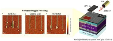 |
| Fig.1: Schematic illustration of direct in-situ high-resolution magnetic imaging using MFM. An ultrashort intense laser pulse is guided through a hollow-core fiber and applied to plasmonic structures deposited on a magnetic multilayer sample. The change in magnetic state probed after irradiation of (a) First laser shot focused on the plasmonic nanobars (superimposed in green). (b) Second laser shot with the same fluence switches the magnetization state back to its original state. (c) Excitation with the third laser pulse reverses the magnetization state at the edge of the nanobars. Credit MBI: T.P.H. Sidiropoulos, P. Singh |
Abstract:
Researchers from Max Born Institute have demonstrated a successful way to control and manipulate nanoscale magnetic bits — the building blocks of digital data — using an ultrafast laser pulse and plasmonic gold nanostructures. The findings were published in Nano Letters.
Ultrafast plasmon-enhanced magnetic bit switching at the nanoscale
Berlin, Germany | Posted on April 25th, 2025All-optical, helicity-independent magnetization switching (AO-HIS) is one of the most interesting and promising mechanisms for this endeavor, where the magnetization state can be reversed between two directions with a single femtosecond laser pulse, serving as “0s” and “1s” without any external magnetic field or complex wiring. This opens up exciting possibilities for creating memory devices that are not only faster and more robust but also consume far less power. Ultrafast light-driven control of magnetization on the nanometer length scale is key to achieve competitive bit sizes in next generation data storage technology. However, it is currently not well understood to what extent basic physics processes such as heat transfer at the nanoscale and the propagation of magnetic domain walls limit the minimum achievable bit size.
To investigate these open questions, the researchers used plasmonic gold nanostructures, which can confine light to regions smaller than the wavelength of light. These structures were fabricated in-house by electron beam lithography on a 10 nm thin film of a magnetic material composed of Rare Earth – Transition Metal alloy (GdTbCo), capable of facilitating small stable magnetic domains due to the presence of the rare earth metal Terbium, generating a large magnetic anisotropy.
Using a 370 fs ultrashort laser pulse of 1030 nm wavelength, magnetic switching was achieved in areas with a width of only 240 nm. The nanostructures also reduced the pulse energies required, due to the enhanced localization of the electromagnetic field around the gold bars, exploiting their plasmonic property.
Illumination with single laser pulses can be used to locally switch the magnetization at the edge of the nanostructure (Fig. 1(a)). Furthermore, a region where the magnetization has been switched by the laser pulse can be reverted with another single laser pulse (Fig. 1(b)) at precisely targeted locations on the magnetic material. It is thus possible to realize a controlled toggling of the magnetization, as required to encode information states “0” and “1”. The final magnetic state was visualized using magnetic force microscopy (MFM), a scanning technique that can image the magnetic state of a sample with nanometer scale spatial resolution.
In addition to the demonstration of toggle switching, under particular laser pulse conditions the researchers observed interesting extended magnetization patterns as shown in Fig. 2. When exciting under conditions where the nanostructures do not allow for a plasmonic resonance to be excited by the laser, a dipole-like far field scattering domain pattern is “imprinted” in the magnetic film. Via on- and off- resonant plasmonic excitation the dominance of different plasmonic energy transfer mechanisms could be studied. “While this is basic research on the fundamental processes of localized optical switching of magnetization, it may guide future developments towards optimized excitation schemes in engineered magnetic materials, ultimately allowing to exploit nanoscale control of magnetism using light”, says Puloma Singh, an MBI researcher driving this project together with her MBI colleagues as part of her PhD studies.
####
For more information, please click here
Contacts:
Media Contact
Alexandra Wettstein
Max Born Institute for Nonlinear Optics and Short Pulse Spectroscopy (MBI)
Office: 0049-30 6392 1402
Expert Contact
Prof. Dr. Stefan Eisebitt
Max Born Institute for Nonlinear Optics and Short Pulse Spectroscopy
Office: +49 30 6392 1300
Copyright © Max Born Institute for Nonlinear Optics and Short Pulse Spectroscopy (MBI)
If you have a comment, please Contact us.Issuers of news releases, not 7th Wave, Inc. or Nanotechnology Now, are solely responsible for the accuracy of the content.
Bookmark:


| Related Links |
| Related News Press |
News and information
![]() Researchers develop molecular qubits that communicate at telecom frequencies October 3rd, 2025
Researchers develop molecular qubits that communicate at telecom frequencies October 3rd, 2025
![]() Next-generation quantum communication October 3rd, 2025
Next-generation quantum communication October 3rd, 2025
![]() "Nanoreactor" cage uses visible light for catalytic and ultra-selective cross-cycloadditions October 3rd, 2025
"Nanoreactor" cage uses visible light for catalytic and ultra-selective cross-cycloadditions October 3rd, 2025
Magnetism/Magnons
![]() Researchers develop molecular qubits that communicate at telecom frequencies October 3rd, 2025
Researchers develop molecular qubits that communicate at telecom frequencies October 3rd, 2025
Possible Futures
![]() Spinel-type sulfide semiconductors to operate the next-generation LEDs and solar cells For solar-cell absorbers and green-LED source October 3rd, 2025
Spinel-type sulfide semiconductors to operate the next-generation LEDs and solar cells For solar-cell absorbers and green-LED source October 3rd, 2025
Chip Technology
![]() Lab to industry: InSe wafer-scale breakthrough for future electronics August 8th, 2025
Lab to industry: InSe wafer-scale breakthrough for future electronics August 8th, 2025
![]() A 1960s idea inspires NBI researchers to study hitherto inaccessible quantum states June 6th, 2025
A 1960s idea inspires NBI researchers to study hitherto inaccessible quantum states June 6th, 2025
![]() Programmable electron-induced color router array May 14th, 2025
Programmable electron-induced color router array May 14th, 2025
Discoveries
![]() Researchers develop molecular qubits that communicate at telecom frequencies October 3rd, 2025
Researchers develop molecular qubits that communicate at telecom frequencies October 3rd, 2025
![]() Next-generation quantum communication October 3rd, 2025
Next-generation quantum communication October 3rd, 2025
![]() "Nanoreactor" cage uses visible light for catalytic and ultra-selective cross-cycloadditions October 3rd, 2025
"Nanoreactor" cage uses visible light for catalytic and ultra-selective cross-cycloadditions October 3rd, 2025
Announcements
![]() Rice membrane extracts lithium from brines with greater speed, less waste October 3rd, 2025
Rice membrane extracts lithium from brines with greater speed, less waste October 3rd, 2025
![]() Researchers develop molecular qubits that communicate at telecom frequencies October 3rd, 2025
Researchers develop molecular qubits that communicate at telecom frequencies October 3rd, 2025
![]() Next-generation quantum communication October 3rd, 2025
Next-generation quantum communication October 3rd, 2025
![]() "Nanoreactor" cage uses visible light for catalytic and ultra-selective cross-cycloadditions October 3rd, 2025
"Nanoreactor" cage uses visible light for catalytic and ultra-selective cross-cycloadditions October 3rd, 2025
Interviews/Book Reviews/Essays/Reports/Podcasts/Journals/White papers/Posters
![]() Spinel-type sulfide semiconductors to operate the next-generation LEDs and solar cells For solar-cell absorbers and green-LED source October 3rd, 2025
Spinel-type sulfide semiconductors to operate the next-generation LEDs and solar cells For solar-cell absorbers and green-LED source October 3rd, 2025
![]() Rice membrane extracts lithium from brines with greater speed, less waste October 3rd, 2025
Rice membrane extracts lithium from brines with greater speed, less waste October 3rd, 2025
|
|
||
|
|
||
| The latest news from around the world, FREE | ||
|
|
||
|
|
||
| Premium Products | ||
|
|
||
|
Only the news you want to read!
Learn More |
||
|
|
||
|
Full-service, expert consulting
Learn More |
||
|
|
||