Home > Press > New technique makes it easier to etch semiconductors
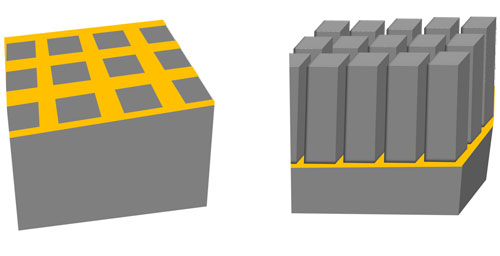 |
| Graphic by Xiuling Li
Metal-assisted chemical etching uses two steps. First, a thin layer of gold is patterned on top of a semiconductor wafer with soft lithography (left). The gold catalyzes a chemical reaction that etches the semiconductor form the top down, creating three-dimensional structures for optoelectronic applications (right). |
Abstract:
Creating semiconductor structures for high-end optoelectronic devices just got easier, thanks to University of Illinois researchers.
New technique makes it easier to etch semiconductors
Posted on December 22nd, 2011The team developed a method to chemically etch patterned arrays in the semiconductor gallium arsenide, used in solar cells, lasers, light emitting diodes (LEDs), field effect transistors (FETs), capacitors and sensors. Led by electrical and computer engineering professor Xiuling Li, the researchers describe their technique in the journal Nano Letters.
A semiconductor's physical properties can vary depending on its structure, so semiconductor wafers are etched into structures that tune their electrical and optical properties and connectivity before they are assembled into chips.
Semiconductors are commonly etched with two techniques: "Wet" etching uses a chemical solution to erode the semiconductor in all directions, while "dry" etching uses a directed beam of ions to bombard the surface, carving out a directed pattern. Such patterns are required for high-aspect-ratio nanostructures, or tiny shapes that have a large ratio of height to width. High-aspect-ratio structures are essential to many high-end optoelectronic device applications.
While silicon is the most ubiquitous material in semiconductor devices, materials in the III-V (pronounced three-five) group are more efficient in optoelectronic applications, such as solar cells or lasers.
Unfortunately, these materials can be difficult to dry etch, as the high-energy ion blasts damage the semiconductor's surface. III-V semiconductors are especially susceptible to damage.
To address this problem, Li and her group turned to metal-assisted chemical etching (MacEtch), a wet-etching approach they had previously developed for silicon. Unlike other wet methods, MacEtch works in one direction, from the top down. It is faster and less expensive than many dry etch techniques, according to Li. Her group revisited the MacEtch technique, optimizing the chemical solution and reaction conditions for the III-V semiconductor gallium arsenide (GaAs).
The process has two steps. First, a thin film of metal is patterned on the GaAs surface. Then, the semiconductor with the metal pattern is immersed in the MacEtch chemical solution. The metal catalyzes the reaction so that only the areas touching metal are etched away, and high-aspect-ratio structures are formed as the metal sinks into the wafer. When the etching is done, the metal can be cleaned from the surface without damaging it.
"It is a big deal to be able to etch GaAs this way," Li said. "The realization of high-aspect-ratio III-V nanostructure arrays by wet etching can potentially transform the fabrication of semiconductor lasers where surface grating is currently fabricated by dry etching, which is expensive and causes surface damage."
To create metal film patterns on the GaAs surface, Li's team used a patterning technique pioneered by John Rogers, the Lee J. Flory-Founder Chair and a professor of materials science and engineering at the U. of I. Their research teams joined forces to optimize the method, called soft lithography, for chemical compatibility while protecting the GaAs surface. Soft lithography is applied to the whole semiconductor wafer, as opposed to small segments, creating patterns over large areas - without expensive optical equipment.
"The combination of soft lithography and MacEtch make the perfect combination to produce large-area, high-aspect-ratio III-V nanostructures in a low-cost fashion," said Li, who is affiliated with the Micro and Nanotechnology Laboratory, the Frederick Seitz Materials Research Laboratory and the Beckman Institute for Advanced Science and Technology at the U. of I.
Next, the researchers hope to further optimize conditions for GaAs etching and establish parameters for MacEtch of other III-V semiconductors. Then, they hope to demonstrate device fabrication, including distributed Bragg reflector lasers and photonic crystals.
"MacEtch is a universal method as long as the right condition for deferential etching with and without metal can be found," Li said.
The Department of Energy and the National Science Foundation supported this work.
####
For more information, please click here
Contacts:
Liz Ahlberg
Physical Sciences Editor
217-244-1073
Xiuling Li
217-265-6354
Copyright © University of Illinois at Urbana-Champaign
If you have a comment, please Contact us.Issuers of news releases, not 7th Wave, Inc. or Nanotechnology Now, are solely responsible for the accuracy of the content.
Bookmark:


| Related Links |
| Related News Press |
News and information
![]() Quantum computer improves AI predictions April 17th, 2026
Quantum computer improves AI predictions April 17th, 2026
![]() Flexible sensor gains sensitivity under pressure April 17th, 2026
Flexible sensor gains sensitivity under pressure April 17th, 2026
![]() A reusable chip for particulate matter sensing April 17th, 2026
A reusable chip for particulate matter sensing April 17th, 2026
![]() Detecting vibrational quantum beating in the predissociation dynamics of SF6 using time-resolved photoelectron spectroscopy April 17th, 2026
Detecting vibrational quantum beating in the predissociation dynamics of SF6 using time-resolved photoelectron spectroscopy April 17th, 2026
Display technology/LEDs/SS Lighting/OLEDs
![]() Spinel-type sulfide semiconductors to operate the next-generation LEDs and solar cells For solar-cell absorbers and green-LED source October 3rd, 2025
Spinel-type sulfide semiconductors to operate the next-generation LEDs and solar cells For solar-cell absorbers and green-LED source October 3rd, 2025
![]() Efficient and stable hybrid perovskite-organic light-emitting diodes with external quantum efficiency exceeding 40 per cent July 5th, 2024
Efficient and stable hybrid perovskite-organic light-emitting diodes with external quantum efficiency exceeding 40 per cent July 5th, 2024
Govt.-Legislation/Regulation/Funding/Policy
![]() Quantum computer improves AI predictions April 17th, 2026
Quantum computer improves AI predictions April 17th, 2026
![]() Metasurfaces smooth light to boost magnetic sensing precision January 30th, 2026
Metasurfaces smooth light to boost magnetic sensing precision January 30th, 2026
![]() New imaging approach transforms study of bacterial biofilms August 8th, 2025
New imaging approach transforms study of bacterial biofilms August 8th, 2025
Chip Technology
![]() A reusable chip for particulate matter sensing April 17th, 2026
A reusable chip for particulate matter sensing April 17th, 2026
![]() Metasurfaces smooth light to boost magnetic sensing precision January 30th, 2026
Metasurfaces smooth light to boost magnetic sensing precision January 30th, 2026
Sensors
![]() Flexible sensor gains sensitivity under pressure April 17th, 2026
Flexible sensor gains sensitivity under pressure April 17th, 2026
![]() Tiny nanosheets, big leap: A new sensor detects ethanol at ultra-low levels January 30th, 2026
Tiny nanosheets, big leap: A new sensor detects ethanol at ultra-low levels January 30th, 2026
![]() From sensors to smart systems: the rise of AI-driven photonic noses January 30th, 2026
From sensors to smart systems: the rise of AI-driven photonic noses January 30th, 2026
![]() Sensors innovations for smart lithium-based batteries: advancements, opportunities, and potential challenges August 8th, 2025
Sensors innovations for smart lithium-based batteries: advancements, opportunities, and potential challenges August 8th, 2025
Nanoelectronics
![]() Lab to industry: InSe wafer-scale breakthrough for future electronics August 8th, 2025
Lab to industry: InSe wafer-scale breakthrough for future electronics August 8th, 2025
![]() Interdisciplinary: Rice team tackles the future of semiconductors Multiferroics could be the key to ultralow-energy computing October 6th, 2023
Interdisciplinary: Rice team tackles the future of semiconductors Multiferroics could be the key to ultralow-energy computing October 6th, 2023
![]() Key element for a scalable quantum computer: Physicists from Forschungszentrum J�lich and RWTH Aachen University demonstrate electron transport on a quantum chip September 23rd, 2022
Key element for a scalable quantum computer: Physicists from Forschungszentrum J�lich and RWTH Aachen University demonstrate electron transport on a quantum chip September 23rd, 2022
![]() Reduced power consumption in semiconductor devices September 23rd, 2022
Reduced power consumption in semiconductor devices September 23rd, 2022
Discoveries
![]() Quantum computer improves AI predictions April 17th, 2026
Quantum computer improves AI predictions April 17th, 2026
![]() Flexible sensor gains sensitivity under pressure April 17th, 2026
Flexible sensor gains sensitivity under pressure April 17th, 2026
![]() A reusable chip for particulate matter sensing April 17th, 2026
A reusable chip for particulate matter sensing April 17th, 2026
![]() Detecting vibrational quantum beating in the predissociation dynamics of SF6 using time-resolved photoelectron spectroscopy April 17th, 2026
Detecting vibrational quantum beating in the predissociation dynamics of SF6 using time-resolved photoelectron spectroscopy April 17th, 2026
Announcements
![]() A fundamentally new therapeutic approach to cystic fibrosis: Nanobody repairs cellular defect April 17th, 2026
A fundamentally new therapeutic approach to cystic fibrosis: Nanobody repairs cellular defect April 17th, 2026
![]() UC Irvine physicists discover method to reverse �quantum scrambling� : The work addresses the problem of information loss in quantum computing system April 17th, 2026
UC Irvine physicists discover method to reverse �quantum scrambling� : The work addresses the problem of information loss in quantum computing system April 17th, 2026
Energy
![]() Sensors innovations for smart lithium-based batteries: advancements, opportunities, and potential challenges August 8th, 2025
Sensors innovations for smart lithium-based batteries: advancements, opportunities, and potential challenges August 8th, 2025
![]() Simple algorithm paired with standard imaging tool could predict failure in lithium metal batteries August 8th, 2025
Simple algorithm paired with standard imaging tool could predict failure in lithium metal batteries August 8th, 2025
Battery Technology/Capacitors/Generators/Piezoelectrics/Thermoelectrics/Energy storage
![]() Decoding hydrogen‑bond network of electrolyte for cryogenic durable aqueous zinc‑ion batteries January 30th, 2026
Decoding hydrogen‑bond network of electrolyte for cryogenic durable aqueous zinc‑ion batteries January 30th, 2026
![]() COF scaffold membrane with gate‑lane nanostructure for efficient Li+/Mg2+ separation January 30th, 2026
COF scaffold membrane with gate‑lane nanostructure for efficient Li+/Mg2+ separation January 30th, 2026
![]() MXene nanomaterials enter a new dimension Multilayer nanomaterial: MXene flakes created at Drexel University show new promise as 1D scrolls January 30th, 2026
MXene nanomaterials enter a new dimension Multilayer nanomaterial: MXene flakes created at Drexel University show new promise as 1D scrolls January 30th, 2026
Solar/Photovoltaic
![]() Spinel-type sulfide semiconductors to operate the next-generation LEDs and solar cells For solar-cell absorbers and green-LED source October 3rd, 2025
Spinel-type sulfide semiconductors to operate the next-generation LEDs and solar cells For solar-cell absorbers and green-LED source October 3rd, 2025
![]() KAIST researchers introduce new and improved, next-generation perovskite solar cell November 8th, 2024
KAIST researchers introduce new and improved, next-generation perovskite solar cell November 8th, 2024
![]() Groundbreaking precision in single-molecule optoelectronics August 16th, 2024
Groundbreaking precision in single-molecule optoelectronics August 16th, 2024
![]() Development of zinc oxide nanopagoda array photoelectrode: photoelectrochemical water-splitting hydrogen production January 12th, 2024
Development of zinc oxide nanopagoda array photoelectrode: photoelectrochemical water-splitting hydrogen production January 12th, 2024
Printing/Lithography/Inkjet/Inks/Bio-printing/Dyes
![]() Presenting: Ultrasound-based printing of 3D materials�potentially inside the body December 8th, 2023
Presenting: Ultrasound-based printing of 3D materials�potentially inside the body December 8th, 2023
![]() Simple ballpoint pen can write custom LEDs August 11th, 2023
Simple ballpoint pen can write custom LEDs August 11th, 2023
![]() Disposable electronics on a simple sheet of paper October 7th, 2022
Disposable electronics on a simple sheet of paper October 7th, 2022
|
|
||
|
|
||
| The latest news from around the world, FREE | ||
|
|
||
|
|
||
| Premium Products | ||
|
|
||
|
Only the news you want to read!
Learn More |
||
|
|
||
|
Full-service, expert consulting
Learn More |
||
|
|
||