Home > Press > CEA-Leti Extends 300mm Line and Adds Avenues for Developing Disruptive Technologies: Execution Relies on CEA-Leti’s Fully Implemented Technology With Module-Level Innovations & Devices and Their Architectures
 |
Abstract:
Leti, a research institute at CEA Tech, today announced during IEDM an extension of its 300mm silicon-based wafer line to open new R&D avenues for its industrial partners. This extension will allow new innovative technological modules to be inserted in, or made compatible with, industrial flows up to completely pioneered technology routes that enable edge AI, HPC, in memory computing, photonics, power electronics and other high-end applications.
CEA-Leti Extends 300mm Line and Adds Avenues for Developing Disruptive Technologies: Execution Relies on CEA-Leti’s Fully Implemented Technology With Module-Level Innovations & Devices and Their Architectures
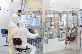
San Francisco, CA | Posted on December 3rd, 2018CEA-Leti’s 300mm wafer-line extension will accelerate innovation projects with fab partners using 300mm wafers.
Targeted technological routes and related targeted applications for the 300mm line extension include:
memory: phase-change RAM (PCRAM), oxide-based resistive memory (OxRAM), conductive-bridging RAM (CBRAM)
vertical image sensors
photonics: III-V on silicon, integrated photonics…
power electronics: insulated-gate bipolar transistors (IGBT)
HPC and edge AI: FD-SOI and derivatives, such as sequential stacking and Si qbits for quantum computing
3D wafer-to-wafer or die-to-wafer bonding, hybrid bonding: substrates and layer transfer for advanced substrates in collaboration with Soitec.
CEA-Leti's advanced CMOS strategy targets FD-SOI research through the development of modules to the economic and technological limits of scaling, and complements the extension of the 300mm platform for edge-AI applications, analog applications, RF and power electronics.
This strategy is based on a mix of priorities of CEA-Leti’s partners and its researchers’ ideas that pioneer enabling technologies to address societal challenges. These include cloud and edge computation, high-volume communication, multi-modality interaction and energy conservation. Leti executes the strategy with its fully implemented technology, from beginning to end with module-level innovations, such as insulation or back-end copper, as well as devices and their architectures.
“Our 300mm line will help Leti continue this strategy by accessing dimensions that make it possible to address the pressing challenges associated with emerging technologies, such as quantum, nanowires and sequential 3D integration,” said Emmanuel Sabonnadičre, CEA-Leti CEO. “CEA-Leti’s industrial partners are now able to develop or test their disruptive technologies and their designs on state-of-the-art equipment, while benefiting from the institute’s R&D expertise, to achieve improved component performance, direct comparison with the ecosystem and easier technology transfers from lab to fab.”
The implementation of this 300mm line is possible thanks to the financing of Auvergne Rhone Alpes region for the acquisition of a 193nm immersion lithography tool, which is the cornerstone of this investment plan (2017-2018). CEA-Leti also benefited from financial support of the French government for the second phase of this plan (2018-2019).
####
About Leti
Leti, a technology research institute at CEA Tech, is a global leader in miniaturization technologies enabling smart, energy-efficient and secure solutions for industry. Founded in 1967, Leti pioneers micro-& nanotechnologies, tailoring differentiating applicative solutions for global companies, SMEs and startups. Leti tackles critical challenges in healthcare, energy and digital migration. From sensors to data processing and computing solutions, Leti’s multidisciplinary teams deliver solid expertise, leveraging world-class pre-industrialization facilities. With a staff of more than 1,900, a portfolio of 2,700 patents, 91,500 sq. ft. of cleanroom space and a clear IP policy, the institute is based in Grenoble, France, and has offices in Silicon Valley and Tokyo. Leti has launched 60 startups and is a member of the Carnot Institutes network. This year, the institute celebrates its 50th anniversary. Follow us on www.leti-cea.com and @CEA_Leti.
Follow us on www.leti.fr/en and @CEA_Leti.
CEA Tech is the technology research branch of the French Alternative Energies and Atomic Energy Commission (CEA), a key player in innovative R&D, defence & security, nuclear energy, technological research for industry and fundamental science, identified by Thomson Reuters as the second most innovative research organization in the world. CEA Tech leverages a unique innovation-driven culture and unrivalled expertise to develop and disseminate new technologies for industry, helping to create high-end products and provide a competitive edge.
For more information, please click here
Contacts:
Press Contact
Agency
+33 6 74 93 23 47
Copyright © Leti
If you have a comment, please Contact us.Issuers of news releases, not 7th Wave, Inc. or Nanotechnology Now, are solely responsible for the accuracy of the content.
Bookmark:


| Related News Press |
News and information
![]() Quantum computer improves AI predictions April 17th, 2026
Quantum computer improves AI predictions April 17th, 2026
![]() Flexible sensor gains sensitivity under pressure April 17th, 2026
Flexible sensor gains sensitivity under pressure April 17th, 2026
![]() A reusable chip for particulate matter sensing April 17th, 2026
A reusable chip for particulate matter sensing April 17th, 2026
![]() Detecting vibrational quantum beating in the predissociation dynamics of SF6 using time-resolved photoelectron spectroscopy April 17th, 2026
Detecting vibrational quantum beating in the predissociation dynamics of SF6 using time-resolved photoelectron spectroscopy April 17th, 2026
Hardware
![]() The present and future of computing get a boost from new research July 21st, 2023
The present and future of computing get a boost from new research July 21st, 2023
![]() A Carbon Nanotube Microprocessor Mature Enough to Say Hello: Three new breakthroughs make commercial nanotube processors possible March 2nd, 2020
A Carbon Nanotube Microprocessor Mature Enough to Say Hello: Three new breakthroughs make commercial nanotube processors possible March 2nd, 2020
![]() Powering the future: Smallest all-digital circuit opens doors to 5 nm next-gen semiconductor February 11th, 2020
Powering the future: Smallest all-digital circuit opens doors to 5 nm next-gen semiconductor February 11th, 2020
Possible Futures
![]() A fundamentally new therapeutic approach to cystic fibrosis: Nanobody repairs cellular defect April 17th, 2026
A fundamentally new therapeutic approach to cystic fibrosis: Nanobody repairs cellular defect April 17th, 2026
![]() UC Irvine physicists discover method to reverse ‘quantum scrambling’ : The work addresses the problem of information loss in quantum computing system April 17th, 2026
UC Irvine physicists discover method to reverse ‘quantum scrambling’ : The work addresses the problem of information loss in quantum computing system April 17th, 2026
Chip Technology
![]() A reusable chip for particulate matter sensing April 17th, 2026
A reusable chip for particulate matter sensing April 17th, 2026
![]() Metasurfaces smooth light to boost magnetic sensing precision January 30th, 2026
Metasurfaces smooth light to boost magnetic sensing precision January 30th, 2026
Quantum Computing
![]() Quantum computer improves AI predictions April 17th, 2026
Quantum computer improves AI predictions April 17th, 2026
![]() UC Irvine physicists discover method to reverse ‘quantum scrambling’ : The work addresses the problem of information loss in quantum computing system April 17th, 2026
UC Irvine physicists discover method to reverse ‘quantum scrambling’ : The work addresses the problem of information loss in quantum computing system April 17th, 2026
![]() Researchers develop molecular qubits that communicate at telecom frequencies October 3rd, 2025
Researchers develop molecular qubits that communicate at telecom frequencies October 3rd, 2025
Sensors
![]() Flexible sensor gains sensitivity under pressure April 17th, 2026
Flexible sensor gains sensitivity under pressure April 17th, 2026
![]() Tiny nanosheets, big leap: A new sensor detects ethanol at ultra-low levels January 30th, 2026
Tiny nanosheets, big leap: A new sensor detects ethanol at ultra-low levels January 30th, 2026
![]() From sensors to smart systems: the rise of AI-driven photonic noses January 30th, 2026
From sensors to smart systems: the rise of AI-driven photonic noses January 30th, 2026
![]() Sensors innovations for smart lithium-based batteries: advancements, opportunities, and potential challenges August 8th, 2025
Sensors innovations for smart lithium-based batteries: advancements, opportunities, and potential challenges August 8th, 2025
Announcements
![]() A fundamentally new therapeutic approach to cystic fibrosis: Nanobody repairs cellular defect April 17th, 2026
A fundamentally new therapeutic approach to cystic fibrosis: Nanobody repairs cellular defect April 17th, 2026
![]() UC Irvine physicists discover method to reverse ‘quantum scrambling’ : The work addresses the problem of information loss in quantum computing system April 17th, 2026
UC Irvine physicists discover method to reverse ‘quantum scrambling’ : The work addresses the problem of information loss in quantum computing system April 17th, 2026
Tools
![]() Metasurfaces smooth light to boost magnetic sensing precision January 30th, 2026
Metasurfaces smooth light to boost magnetic sensing precision January 30th, 2026
![]() From sensors to smart systems: the rise of AI-driven photonic noses January 30th, 2026
From sensors to smart systems: the rise of AI-driven photonic noses January 30th, 2026
![]() Japan launches fully domestically produced quantum computer: Expo visitors to experience quantum computing firsthand August 8th, 2025
Japan launches fully domestically produced quantum computer: Expo visitors to experience quantum computing firsthand August 8th, 2025
Industrial
![]() Tiny nanosheets, big leap: A new sensor detects ethanol at ultra-low levels January 30th, 2026
Tiny nanosheets, big leap: A new sensor detects ethanol at ultra-low levels January 30th, 2026
![]() Quantum interference in molecule-surface collisions February 28th, 2025
Quantum interference in molecule-surface collisions February 28th, 2025
![]() Boron nitride nanotube fibers get real: Rice lab creates first heat-tolerant, stable fibers from wet-spinning process June 24th, 2022
Boron nitride nanotube fibers get real: Rice lab creates first heat-tolerant, stable fibers from wet-spinning process June 24th, 2022
Artificial Intelligence
![]() Quantum computer improves AI predictions April 17th, 2026
Quantum computer improves AI predictions April 17th, 2026
![]() From sensors to smart systems: the rise of AI-driven photonic noses January 30th, 2026
From sensors to smart systems: the rise of AI-driven photonic noses January 30th, 2026
![]() New quantum encoding methods slash circuit complexity in machine learning November 8th, 2024
New quantum encoding methods slash circuit complexity in machine learning November 8th, 2024
Photonics/Optics/Lasers
![]() Metasurfaces smooth light to boost magnetic sensing precision January 30th, 2026
Metasurfaces smooth light to boost magnetic sensing precision January 30th, 2026
![]() From sensors to smart systems: the rise of AI-driven photonic noses January 30th, 2026
From sensors to smart systems: the rise of AI-driven photonic noses January 30th, 2026
Printing/Lithography/Inkjet/Inks/Bio-printing/Dyes
![]() Presenting: Ultrasound-based printing of 3D materials—potentially inside the body December 8th, 2023
Presenting: Ultrasound-based printing of 3D materials—potentially inside the body December 8th, 2023
![]() Simple ballpoint pen can write custom LEDs August 11th, 2023
Simple ballpoint pen can write custom LEDs August 11th, 2023
![]() Disposable electronics on a simple sheet of paper October 7th, 2022
Disposable electronics on a simple sheet of paper October 7th, 2022
|
|
||
|
|
||
| The latest news from around the world, FREE | ||
|
|
||
|
|
||
| Premium Products | ||
|
|
||
|
Only the news you want to read!
Learn More |
||
|
|
||
|
Full-service, expert consulting
Learn More |
||
|
|
||