Home > Press > Graphene forged into three-dimensional shapes
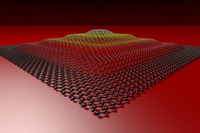 |
| A similar structure was made experimentally by using laser irradiation in a process called "optical forging." CREDIT The University of Jyv�skyl� |
Abstract:
Researchers from Finland and Taiwan have discovered how graphene, a single-atom-thin layer of carbon, can be forged into three-dimensional objects by using laser light. A striking illustration was provided when the researchers fabricated a pyramid with a height of 60 nm, which is about 200 times larger than the thickness of a graphene sheet. The pyramid was so small that it would easily fit on a single strand of hair. The research was supported by the Academy of Finland and the Ministry of Science and Technology of the Republic of China.
Graphene forged into three-dimensional shapes
Helsinki, Finland | Posted on September 26th, 2017Graphene is a close relative to graphite, which consists of millions of layers of graphene and can be found in common pencil tips. After graphene was first isolated in 2004, researchers have learned to routinely produce and handle it. Graphene can be used to make electronic and optoelectronic devices, such as transistors, photodetectors and sensors. In future, we will probably see an increasing number of products containing graphene.
"We call this technique optical forging, since the process resembles forging metals into 3D shapes with a hammer. In our case, a laser beam is the hammer that forges graphene into 3D shapes," explains Professor Mika Pettersson, who led the experimental team at the Nanoscience Center of the University of Jyv�skyl�, Finland. "The beauty of the technique is that it's fast and easy to use; it doesn't require any additional chemicals or processing. Despite the simplicity of the technique, we were very surprised initially when we observed that the laser beam induced such substantial changes on graphene. It took a while to understand what was happening."
"At first, we were flabbergasted. The experimental data simply made no sense," says Dr Pekka Koskinen, who was responsible for the theory. "But gradually, by close interplay between experiments and computer simulations, the actuality of 3D shapes and their formation mechanism started to become clear."
"When we first examined the irradiated graphene, we were expecting to find traces of chemical species incorporated into the graphene, but we couldn't find any. After some more careful inspections, we concluded that it must be purely structural defects, rather than chemical doping, that are responsible for such dramatic changes on graphene," explains Associate Professor Wei Yen Woon from Taiwan, who led the experimental group that carried out X-ray photoelectron spectroscopy at the synchrotron facility.
The novel 3D graphene is stable and it has electronic and optical properties that differ from normal 2D graphene. Optically forged graphene can help in fabricating 3D architectures for graphene-based devices.
###
The research was carried out at the Nanoscience Center (NSC) of the University of Jyv�skyl�, the National Central University of Taiwan and the National Synchrotron Radiation Research Center in Taiwan.
####
For more information, please click here
Contacts:
Mika Pettersson
358-503-109-969
Associate Professor
Wei Yen Woon
tel. +886 927 374 826
Copyright © Academy of Finland
If you have a comment, please Contact us.Issuers of news releases, not 7th Wave, Inc. or Nanotechnology Now, are solely responsible for the accuracy of the content.
Bookmark:


| Related Links |
| Related News Press |
News and information
![]() Quantum computer improves AI predictions April 17th, 2026
Quantum computer improves AI predictions April 17th, 2026
![]() Flexible sensor gains sensitivity under pressure April 17th, 2026
Flexible sensor gains sensitivity under pressure April 17th, 2026
![]() A reusable chip for particulate matter sensing April 17th, 2026
A reusable chip for particulate matter sensing April 17th, 2026
![]() Detecting vibrational quantum beating in the predissociation dynamics of SF6 using time-resolved photoelectron spectroscopy April 17th, 2026
Detecting vibrational quantum beating in the predissociation dynamics of SF6 using time-resolved photoelectron spectroscopy April 17th, 2026
2 Dimensional Materials
![]() Flexible sensor gains sensitivity under pressure April 17th, 2026
Flexible sensor gains sensitivity under pressure April 17th, 2026
Graphene/ Graphite
![]() Electrifying results shed light on graphene foam as a potential material for lab grown cartilage June 6th, 2025
Electrifying results shed light on graphene foam as a potential material for lab grown cartilage June 6th, 2025
![]() Breakthrough in proton barrier films using pore-free graphene oxide: Kumamoto University researchers achieve new milestone in advanced coating technologies September 13th, 2024
Breakthrough in proton barrier films using pore-free graphene oxide: Kumamoto University researchers achieve new milestone in advanced coating technologies September 13th, 2024
Possible Futures
![]() A fundamentally new therapeutic approach to cystic fibrosis: Nanobody repairs cellular defect April 17th, 2026
A fundamentally new therapeutic approach to cystic fibrosis: Nanobody repairs cellular defect April 17th, 2026
![]() UC Irvine physicists discover method to reverse �quantum scrambling� : The work addresses the problem of information loss in quantum computing system April 17th, 2026
UC Irvine physicists discover method to reverse �quantum scrambling� : The work addresses the problem of information loss in quantum computing system April 17th, 2026
Discoveries
![]() Quantum computer improves AI predictions April 17th, 2026
Quantum computer improves AI predictions April 17th, 2026
![]() Flexible sensor gains sensitivity under pressure April 17th, 2026
Flexible sensor gains sensitivity under pressure April 17th, 2026
![]() A reusable chip for particulate matter sensing April 17th, 2026
A reusable chip for particulate matter sensing April 17th, 2026
![]() Detecting vibrational quantum beating in the predissociation dynamics of SF6 using time-resolved photoelectron spectroscopy April 17th, 2026
Detecting vibrational quantum beating in the predissociation dynamics of SF6 using time-resolved photoelectron spectroscopy April 17th, 2026
Materials/Metamaterials/Magnetoresistance
![]() First real-time observation of two-dimensional melting process: Researchers at Mainz University unveil new insights into magnetic vortex structures August 8th, 2025
First real-time observation of two-dimensional melting process: Researchers at Mainz University unveil new insights into magnetic vortex structures August 8th, 2025
![]() Researchers unveil a groundbreaking clay-based solution to capture carbon dioxide and combat climate change June 6th, 2025
Researchers unveil a groundbreaking clay-based solution to capture carbon dioxide and combat climate change June 6th, 2025
![]() A 1960s idea inspires NBI researchers to study hitherto inaccessible quantum states June 6th, 2025
A 1960s idea inspires NBI researchers to study hitherto inaccessible quantum states June 6th, 2025
![]() Institute for Nanoscience hosts annual proposal planning meeting May 16th, 2025
Institute for Nanoscience hosts annual proposal planning meeting May 16th, 2025
Announcements
![]() A fundamentally new therapeutic approach to cystic fibrosis: Nanobody repairs cellular defect April 17th, 2026
A fundamentally new therapeutic approach to cystic fibrosis: Nanobody repairs cellular defect April 17th, 2026
![]() UC Irvine physicists discover method to reverse �quantum scrambling� : The work addresses the problem of information loss in quantum computing system April 17th, 2026
UC Irvine physicists discover method to reverse �quantum scrambling� : The work addresses the problem of information loss in quantum computing system April 17th, 2026
Interviews/Book Reviews/Essays/Reports/Podcasts/Journals/White papers/Posters
![]() A fundamentally new therapeutic approach to cystic fibrosis: Nanobody repairs cellular defect April 17th, 2026
A fundamentally new therapeutic approach to cystic fibrosis: Nanobody repairs cellular defect April 17th, 2026
![]() UC Irvine physicists discover method to reverse �quantum scrambling� : The work addresses the problem of information loss in quantum computing system April 17th, 2026
UC Irvine physicists discover method to reverse �quantum scrambling� : The work addresses the problem of information loss in quantum computing system April 17th, 2026
Tools
![]() Metasurfaces smooth light to boost magnetic sensing precision January 30th, 2026
Metasurfaces smooth light to boost magnetic sensing precision January 30th, 2026
![]() From sensors to smart systems: the rise of AI-driven photonic noses January 30th, 2026
From sensors to smart systems: the rise of AI-driven photonic noses January 30th, 2026
![]() Japan launches fully domestically produced quantum computer: Expo visitors to experience quantum computing firsthand August 8th, 2025
Japan launches fully domestically produced quantum computer: Expo visitors to experience quantum computing firsthand August 8th, 2025
Photonics/Optics/Lasers
![]() Metasurfaces smooth light to boost magnetic sensing precision January 30th, 2026
Metasurfaces smooth light to boost magnetic sensing precision January 30th, 2026
![]() From sensors to smart systems: the rise of AI-driven photonic noses January 30th, 2026
From sensors to smart systems: the rise of AI-driven photonic noses January 30th, 2026
|
|
||
|
|
||
| The latest news from around the world, FREE | ||
|
|
||
|
|
||
| Premium Products | ||
|
|
||
|
Only the news you want to read!
Learn More |
||
|
|
||
|
Full-service, expert consulting
Learn More |
||
|
|
||