Home > Press > Movies of graphene nanopore opening
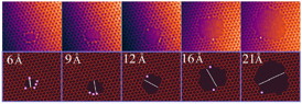 |
| Figure: Nanopores in graphene, catalyzed by single silicon atoms and recorded by HTEM. Source: http://www.graphenea.com/blogs/graphene-news/12040077-movies-of-graphene-nanopore-opening#ixzz2tPrSBi3U |
Abstract:
Fabricating functional nano-devices is an ultimate goal of nanotechnology. Atomic-scale modification and sculpting of materials can enable nano-machines with wide-varying application potential in biological (medical) and chemical (trace sensing) uses. In our most recent publication, together with Harvard University, the Lawrence Berkeley National Laboratory and FEI corporation, we demonstrate precise modification of graphene at the atomic scale.
Movies of graphene nanopore opening
San Sebastian, Spain | Posted on February 15th, 2014In our paper "Direct Observation of a Long-Lived Single-Atom Catalyst Chiseling Atomic Structures in Graphene", published in NanoLetters, we report the direct observation of single silicon atoms catalyzing a reaction on a graphene surface. The reaction removes carbon atoms in a controlled fashion, allowing for precise sculpting of nanopores in graphene. Nanopores in graphene hold great technological and scientific potential, and are already being considered for several uses, such as water filtration and DNA sequencing.
Known to humans for centuries, catalysts play an enabling role in many chemical processes that are important to the modern society. Recent advances in nanotechnology introduced nanocatalysts that enable the creation of novel nanostructures, such as carbon nanotubes and semiconductor nanowires. The characteristics of the resulting structures can be tuned by the structures of the corresponding nanocatalysts. For example, in the growth of semiconductor nanowires from metal nanoparticles, the diameter of the resultant nanowire is determined by the size of the catalytic nanoparticles.
Catalysis typically involves complex atomic-scale events that are hard to record, either because they are too fast or too small for the instrumentation used for the recording. We overcome these challenges by using high-resolution transmission electron microscopy (HRTEM) to record individual silicon atoms as they catalyze the graphene chiseling reaction. The products of the chiseling process are atomic-scale features including graphene pores and clean edges.
The silicon atoms are naturally present impurities in the HRTEM chamber. The atoms freely drift along the graphene surface, until they come across an occasional atomic-scale defect in the sheet. The silicon atom then replaces a carbon atom in the chickenwire structure of graphene. A scientist starts the chiseling reaction by directing a focused electron beam to the defect site. The width of the pore starts from only a few angstroms, gradually increasing with the presence of silicon adatoms and under continuous electron irradiation. The pore size is controlled by stopping the irradiation when the desired size has been reached, as seen in the figure above.
These molecular-sized pores are excellent candidates for molecular detection applications, such as rapid DNA sequencing, because they can be tuned to match the size of a single DNA molecule (~10 Angstroms) for the sensitivity that is needed for single base recognition.
Apart from demonstrating the proof of principle, we found some interesting physics of the process, including the dynamics, stability and selectivity of the single-atom chiseling process. Our findings show that there are likely other pairs of atoms in nature, aside from silicon-graphene, that possess atomic chiseling ability.
The graphene used in this research is our standard high-quality CVD graphene, transferred onto a TEM grid.
####
About Graphenea
We are a leading graphene company that manufacture, produce and supply graphene for industrial and research needs. We have developed a synthesis and transfer process to obtain high uniformity monolayer graphene films on any substrate.
For more information, please click here
Contacts:
General Enquiries
Copyright © Graphenea
If you have a comment, please Contact us.Issuers of news releases, not 7th Wave, Inc. or Nanotechnology Now, are solely responsible for the accuracy of the content.
Bookmark:


| Related Links |
| Related News Press |
News and information
![]() Quantum computer improves AI predictions April 17th, 2026
Quantum computer improves AI predictions April 17th, 2026
![]() Flexible sensor gains sensitivity under pressure April 17th, 2026
Flexible sensor gains sensitivity under pressure April 17th, 2026
![]() A reusable chip for particulate matter sensing April 17th, 2026
A reusable chip for particulate matter sensing April 17th, 2026
![]() Detecting vibrational quantum beating in the predissociation dynamics of SF6 using time-resolved photoelectron spectroscopy April 17th, 2026
Detecting vibrational quantum beating in the predissociation dynamics of SF6 using time-resolved photoelectron spectroscopy April 17th, 2026
Physics
![]() UC Irvine physicists discover method to reverse �quantum scrambling� : The work addresses the problem of information loss in quantum computing system April 17th, 2026
UC Irvine physicists discover method to reverse �quantum scrambling� : The work addresses the problem of information loss in quantum computing system April 17th, 2026
![]() Quantum computers simulate fundamental physics: shedding light on the building blocks of nature June 6th, 2025
Quantum computers simulate fundamental physics: shedding light on the building blocks of nature June 6th, 2025
![]() A 1960s idea inspires NBI researchers to study hitherto inaccessible quantum states June 6th, 2025
A 1960s idea inspires NBI researchers to study hitherto inaccessible quantum states June 6th, 2025
![]() Magnetism in new exotic material opens the way for robust quantum computers June 4th, 2025
Magnetism in new exotic material opens the way for robust quantum computers June 4th, 2025
Videos/Movies
![]() ICFO researchers overcome long-standing bottleneck in single photon detection with twisted 2D materials August 8th, 2025
ICFO researchers overcome long-standing bottleneck in single photon detection with twisted 2D materials August 8th, 2025
Graphene/ Graphite
![]() Electrifying results shed light on graphene foam as a potential material for lab grown cartilage June 6th, 2025
Electrifying results shed light on graphene foam as a potential material for lab grown cartilage June 6th, 2025
Announcements
![]() A fundamentally new therapeutic approach to cystic fibrosis: Nanobody repairs cellular defect April 17th, 2026
A fundamentally new therapeutic approach to cystic fibrosis: Nanobody repairs cellular defect April 17th, 2026
![]() UC Irvine physicists discover method to reverse �quantum scrambling� : The work addresses the problem of information loss in quantum computing system April 17th, 2026
UC Irvine physicists discover method to reverse �quantum scrambling� : The work addresses the problem of information loss in quantum computing system April 17th, 2026
Interviews/Book Reviews/Essays/Reports/Podcasts/Journals/White papers/Posters
![]() A fundamentally new therapeutic approach to cystic fibrosis: Nanobody repairs cellular defect April 17th, 2026
A fundamentally new therapeutic approach to cystic fibrosis: Nanobody repairs cellular defect April 17th, 2026
![]() UC Irvine physicists discover method to reverse �quantum scrambling� : The work addresses the problem of information loss in quantum computing system April 17th, 2026
UC Irvine physicists discover method to reverse �quantum scrambling� : The work addresses the problem of information loss in quantum computing system April 17th, 2026
Water
![]() Taking salt out of the water equation October 7th, 2022
Taking salt out of the water equation October 7th, 2022
|
|
||
|
|
||
| The latest news from around the world, FREE | ||
|
|
||
|
|
||
| Premium Products | ||
|
|
||
|
Only the news you want to read!
Learn More |
||
|
|
||
|
Full-service, expert consulting
Learn More |
||
|
|
||