Home > Press > How to grow wires and tiny plates Liquid processing method developed at MIT can control the shapes of nanowires and produce complete electronic devices
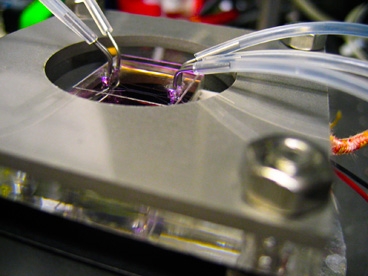 |
| Nanostructures are directly synthesized in parallel microfluidic channels (held by the metal frame) by flowing special chemical reactant solution through the tubing. The microfluidic not only creates the functional device, but is also the final packaged functional LED device itself. Photo: Jaebum Joo |
Abstract:
Researchers at MIT have found a way to control precisely the shapes of submicroscopic wires deposited from a solution — using a method that makes it possible to produce entire electronic devices through a liquid-based process.
How to grow wires and tiny plates Liquid processing method developed at MIT can control the shapes of nanowires and produce complete electronic devices
Cambridge, MA | Posted on July 14th, 2011The team demonstrated the technique by producing a functional light-emitting diode (LED) array made of zinc oxide nanowires in a single beaker, instead of the several separate steps and devices required for conventional production. They were able to do so under relatively benign conditions, with moderate temperatures and no vacuum needed.
Unlike larger structures, with nanomaterials — those with dimensions measured in nanometers, or billionths of a meter — differences in shape can lead to dramatic differences in behavior. "For nanostructures, there's a coupling between the geometry and the electrical and optical properties," explains Brian Chow, a postdoc at MIT and co-author of a paper describing the results that was published July 10 in the journal Nature Materials. "Being able to tune the geometry is very powerful," he says. The system Chow and his colleagues developed can precisely control the aspect ratio (the ratio of length to width) of the nanowires to produce anything from flat plates to long thin wires.
There are other ways of making such nanowires, Chow says. "People have done a good job of controlling the morphology of wires by other means — using high temperatures, high pressure, or subtractive processing. But to be able to do this under these benign conditions is attractive," because it makes it possible to integrate such devices with relatively fragile materials such as polymers and plastics, he says.
Control over the shapes of the wires has until now been essentially a trial-and-error process. "We were trying to find out what is the controlling factor," explains Jaebum Joo PhD '10, who was the lead author of the paper.
The key turns out to be the electrostatic properties of the zinc oxide material as it grows from a solution, they found. Different compounds, when added to the solution, attach themselves electrostatically only to certain parts of the wire — just to the sides, or just to the ends — inhibiting the wire's growth in those directions. The amount of inhibition depends on the specific properties of the added compounds.
While this work was done with zinc oxide nanowires — a promising material that is being widely studied by researchers — the MIT scientists believe the method they developed for controlling the shape of the wires "can be expanded to different material systems," Joo says, perhaps including titanium dioxide which is being investigated for devices such as solar cells. Because the benign assembly conditions allow the material to be deposited on plastic surfaces, he says, it might enable the development of flexible display panels, for example.
But there are also many potential applications using the zinc oxide material itself, including the production of batteries, sensors, and optical devices. And the processing method has "the potential for large-scale manufacturing," Joo says.
The team also hopes to be able to use the method to make "spatially complex devices from the bottom up, out of biocompatible polymers." These could be used, for example, to make tiny devices that could be implanted in the brain to provide both sensing and stimulation.
In addition to Joo and Chow, the research was carried out by visiting scholar Manu Prakesh, along with Media Lab associate professors Edward Boyden and Joseph Jacobson. It was funded by the MIT Center for Bits and Atoms; the MIT Media Lab; the Korea Foundation for Advanced Studies; Samsung Electronics; the Harvard Society of Fellows; the Wallace H. Coulter Early Career Award; the NARSAD Young Investigator Award; the National Science Foundation; and the NIH Director's New Innovator Award.
####
For more information, please click here
Copyright © MIT
If you have a comment, please Contact us.Issuers of news releases, not 7th Wave, Inc. or Nanotechnology Now, are solely responsible for the accuracy of the content.
Bookmark:


| Related News Press |
News and information
![]() Quantum computer improves AI predictions April 17th, 2026
Quantum computer improves AI predictions April 17th, 2026
![]() Flexible sensor gains sensitivity under pressure April 17th, 2026
Flexible sensor gains sensitivity under pressure April 17th, 2026
![]() A reusable chip for particulate matter sensing April 17th, 2026
A reusable chip for particulate matter sensing April 17th, 2026
![]() Detecting vibrational quantum beating in the predissociation dynamics of SF6 using time-resolved photoelectron spectroscopy April 17th, 2026
Detecting vibrational quantum beating in the predissociation dynamics of SF6 using time-resolved photoelectron spectroscopy April 17th, 2026
Display technology/LEDs/SS Lighting/OLEDs
![]() Spinel-type sulfide semiconductors to operate the next-generation LEDs and solar cells For solar-cell absorbers and green-LED source October 3rd, 2025
Spinel-type sulfide semiconductors to operate the next-generation LEDs and solar cells For solar-cell absorbers and green-LED source October 3rd, 2025
![]() Efficient and stable hybrid perovskite-organic light-emitting diodes with external quantum efficiency exceeding 40 per cent July 5th, 2024
Efficient and stable hybrid perovskite-organic light-emitting diodes with external quantum efficiency exceeding 40 per cent July 5th, 2024
Govt.-Legislation/Regulation/Funding/Policy
![]() Quantum computer improves AI predictions April 17th, 2026
Quantum computer improves AI predictions April 17th, 2026
![]() Metasurfaces smooth light to boost magnetic sensing precision January 30th, 2026
Metasurfaces smooth light to boost magnetic sensing precision January 30th, 2026
![]() New imaging approach transforms study of bacterial biofilms August 8th, 2025
New imaging approach transforms study of bacterial biofilms August 8th, 2025
Sensors
![]() Flexible sensor gains sensitivity under pressure April 17th, 2026
Flexible sensor gains sensitivity under pressure April 17th, 2026
![]() Tiny nanosheets, big leap: A new sensor detects ethanol at ultra-low levels January 30th, 2026
Tiny nanosheets, big leap: A new sensor detects ethanol at ultra-low levels January 30th, 2026
![]() From sensors to smart systems: the rise of AI-driven photonic noses January 30th, 2026
From sensors to smart systems: the rise of AI-driven photonic noses January 30th, 2026
![]() Sensors innovations for smart lithium-based batteries: advancements, opportunities, and potential challenges August 8th, 2025
Sensors innovations for smart lithium-based batteries: advancements, opportunities, and potential challenges August 8th, 2025
Nanoelectronics
![]() Lab to industry: InSe wafer-scale breakthrough for future electronics August 8th, 2025
Lab to industry: InSe wafer-scale breakthrough for future electronics August 8th, 2025
![]() Interdisciplinary: Rice team tackles the future of semiconductors Multiferroics could be the key to ultralow-energy computing October 6th, 2023
Interdisciplinary: Rice team tackles the future of semiconductors Multiferroics could be the key to ultralow-energy computing October 6th, 2023
![]() Key element for a scalable quantum computer: Physicists from Forschungszentrum Jülich and RWTH Aachen University demonstrate electron transport on a quantum chip September 23rd, 2022
Key element for a scalable quantum computer: Physicists from Forschungszentrum Jülich and RWTH Aachen University demonstrate electron transport on a quantum chip September 23rd, 2022
![]() Reduced power consumption in semiconductor devices September 23rd, 2022
Reduced power consumption in semiconductor devices September 23rd, 2022
Discoveries
![]() Quantum computer improves AI predictions April 17th, 2026
Quantum computer improves AI predictions April 17th, 2026
![]() Flexible sensor gains sensitivity under pressure April 17th, 2026
Flexible sensor gains sensitivity under pressure April 17th, 2026
![]() A reusable chip for particulate matter sensing April 17th, 2026
A reusable chip for particulate matter sensing April 17th, 2026
![]() Detecting vibrational quantum beating in the predissociation dynamics of SF6 using time-resolved photoelectron spectroscopy April 17th, 2026
Detecting vibrational quantum beating in the predissociation dynamics of SF6 using time-resolved photoelectron spectroscopy April 17th, 2026
Announcements
![]() A fundamentally new therapeutic approach to cystic fibrosis: Nanobody repairs cellular defect April 17th, 2026
A fundamentally new therapeutic approach to cystic fibrosis: Nanobody repairs cellular defect April 17th, 2026
![]() UC Irvine physicists discover method to reverse ‘quantum scrambling’ : The work addresses the problem of information loss in quantum computing system April 17th, 2026
UC Irvine physicists discover method to reverse ‘quantum scrambling’ : The work addresses the problem of information loss in quantum computing system April 17th, 2026
Battery Technology/Capacitors/Generators/Piezoelectrics/Thermoelectrics/Energy storage
![]() Decoding hydrogen‑bond network of electrolyte for cryogenic durable aqueous zinc‑ion batteries January 30th, 2026
Decoding hydrogen‑bond network of electrolyte for cryogenic durable aqueous zinc‑ion batteries January 30th, 2026
![]() COF scaffold membrane with gate‑lane nanostructure for efficient Li+/Mg2+ separation January 30th, 2026
COF scaffold membrane with gate‑lane nanostructure for efficient Li+/Mg2+ separation January 30th, 2026
![]() MXene nanomaterials enter a new dimension Multilayer nanomaterial: MXene flakes created at Drexel University show new promise as 1D scrolls January 30th, 2026
MXene nanomaterials enter a new dimension Multilayer nanomaterial: MXene flakes created at Drexel University show new promise as 1D scrolls January 30th, 2026
Photonics/Optics/Lasers
![]() Metasurfaces smooth light to boost magnetic sensing precision January 30th, 2026
Metasurfaces smooth light to boost magnetic sensing precision January 30th, 2026
![]() From sensors to smart systems: the rise of AI-driven photonic noses January 30th, 2026
From sensors to smart systems: the rise of AI-driven photonic noses January 30th, 2026
|
|
||
|
|
||
| The latest news from around the world, FREE | ||
|
|
||
|
|
||
| Premium Products | ||
|
|
||
|
Only the news you want to read!
Learn More |
||
|
|
||
|
Full-service, expert consulting
Learn More |
||
|
|
||