Home > Press > Silicon-graphene hybrid plasmonic waveguide photodetectors beyond 1.55 μm
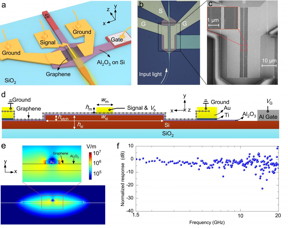 |
| a. Schematic configuration; b. Optical microscope; c. SEM pictures; d. Cross-section of the present silicon-graphene hybrid plasmonic waveguide with the signal electrode at the middle and the ground electrodes at both sides (here the metal-graphene-metal sandwich structure is utilized); e. The electric field component distribution of the quasi-TE0 mode for the optimized silicon-graphene hybrid plasmonic waveguide; f. Measured frequency response of Device B operating at ��=2μm (bias voltage: -0.5 V, gate voltage: 2.9 V). CREDIT Jingshu Guo, Jiang Li, Chaoyue Liu, Yanlong Yin, Wenhui Wang, Zhenhua Ni, Zhilei Fu, Hui Yu, Yang Xu, Yaocheng Shi, Yungui Ma, Shiming Gao, Liming Tong and Daoxin Dai |
Abstract:
Silicon photonics is known as a key technology for modern optical communications at the near infrared wavelength-band, i.e., 1.31/1.55 μm. Currently silicon photonics has been desired to be extended to the wavelength-band beyond 1.55 μm, e.g., 2 μm, for important applications in optical communications, nonlinear photonics, and on-chip sensing. However, the realization of high-performance silicon-based waveguide photodetectors beyond 1.55 μm still faces challenges since there are some fabrication issues as well as wavelength-band limitations. As an alternative, two-dimensional materials (e.g., graphene) provide a promising solution because of the ability for broad operation wavelength-bands and the advantage of avoiding structure mismatch in the design and fabrication.
Silicon-graphene hybrid plasmonic waveguide photodetectors beyond 1.55 μm
Changchun, China | Posted on March 13th, 2020In the paper published in Light: Science & Applications, scientists from Zhejiang University and Southeast University in China proposed and demonstrated high-performance waveguide photodetectors beyond 1.55 μm by introducing a novel silicon-graphene hybrid plasmonic waveguide. In particular, an ultra-thin wide silicon ridge core region with a metal cap atop is introduced to obtain a unique mode field profile, so that light absorption of graphene is enhanced. Furthermore, the fabrication is easy and the graphene-metal contact resistance is reduced, compared to the previous silicon-graphene hybrid waveguides. For example, the graphene absorption efficiencies are as high as 54.3% and 68.6% for 20 μm-long and 50 μm-long absorption regions, when operating at 1.55 μm and 2 μm, respectively.
For the fabricated photodetectors operating at 2 μm, the measured 3 dB-bandwidths are >20 GHz (limited by the experimental setup), while the responsivities are 30-70 mA/W for 0.28 mW input optical power under -0.3V bias voltage. For the photodetectors operating at 1.55 μm, the 3 dB-bandwidth is >40 GHz (limited by the setup), while the measured responsivity is about 0.4 A/W for 0.16 mW input optical power under -0.3V bias voltage.
In this work, the mechanisms in graphene photodetectors are analyzed carefully, which suggested that the photo-thermoelectric effect is the dominant mechanism for photo-response when operating at zero bias voltage. When the photodetector operates at non-zero bias voltages, the dominant mechanism becomes the bolometric or photoconductive effect. This comprehensive analysis helps better understand the photocurrent generation in the graphene-metal interfaces.
These scientists summarize the highlights of their work:
"We have proposed and demonstrated high-performance silicon-graphene hybrid plasmonic waveguide photodetectors beyond 1.55 μm. In particular, a novel silicon-graphene hybrid plasmonic waveguide was used by introducing an ultra-thin wide silicon ridge core region with a metal cap atop. The optical modal filed is manipulated in both vertical and horizontal directions. Thus, the light absorption in graphene is enhanced, meanwhile the metal absorption loss is minimized. This greatly helps achieve sufficient light absorption of graphene within a short absorption region."
"The silicon-graphene waveguide photodetectors operating at 2 μm were demonstrated with a 3 dB-bandwidth over 20 GHz. The measured responsivity is 30-70 mA/W at the bias voltage of -0.3V for input optical power of 0.28 mW. The photodetector at 1.55 μm was also demonstrated with excellent performances. The present work paves the way for achieving high-responsivity and high-speed waveguide photodetectors on silicon for near/mid-infrared wavelength-bands" they added.
"In future works, more efforts should be given to introduce some special junction structures to minimize the dark current and further extend the operation wavelength-band. Graphene waveguide photodetectors may play an important role in mid-infrared silicon photonics, which will play an important role in time resolved spectroscopy, lab-on-chip sensing, nonlinear photonics, as well as optical communication" they said.
####
For more information, please click here
Contacts:
Daoxin Dai
Copyright © Changchun Institute of Optics, Fine Mechanics and Physics, Chinese Academy of Sciences
If you have a comment, please Contact us.Issuers of news releases, not 7th Wave, Inc. or Nanotechnology Now, are solely responsible for the accuracy of the content.
Bookmark:


| Related Links |
| Related News Press |
News and information
![]() Quantum computer improves AI predictions April 17th, 2026
Quantum computer improves AI predictions April 17th, 2026
![]() Flexible sensor gains sensitivity under pressure April 17th, 2026
Flexible sensor gains sensitivity under pressure April 17th, 2026
![]() A reusable chip for particulate matter sensing April 17th, 2026
A reusable chip for particulate matter sensing April 17th, 2026
![]() Detecting vibrational quantum beating in the predissociation dynamics of SF6 using time-resolved photoelectron spectroscopy April 17th, 2026
Detecting vibrational quantum beating in the predissociation dynamics of SF6 using time-resolved photoelectron spectroscopy April 17th, 2026
Imaging
![]() Simple algorithm paired with standard imaging tool could predict failure in lithium metal batteries August 8th, 2025
Simple algorithm paired with standard imaging tool could predict failure in lithium metal batteries August 8th, 2025
![]() First real-time observation of two-dimensional melting process: Researchers at Mainz University unveil new insights into magnetic vortex structures August 8th, 2025
First real-time observation of two-dimensional melting process: Researchers at Mainz University unveil new insights into magnetic vortex structures August 8th, 2025
![]() New imaging approach transforms study of bacterial biofilms August 8th, 2025
New imaging approach transforms study of bacterial biofilms August 8th, 2025
Wireless/telecommunications/RF/Antennas/Microwaves
![]() Researchers develop molecular qubits that communicate at telecom frequencies October 3rd, 2025
Researchers develop molecular qubits that communicate at telecom frequencies October 3rd, 2025
Graphene/ Graphite
![]() Electrifying results shed light on graphene foam as a potential material for lab grown cartilage June 6th, 2025
Electrifying results shed light on graphene foam as a potential material for lab grown cartilage June 6th, 2025
![]() Breakthrough in proton barrier films using pore-free graphene oxide: Kumamoto University researchers achieve new milestone in advanced coating technologies September 13th, 2024
Breakthrough in proton barrier films using pore-free graphene oxide: Kumamoto University researchers achieve new milestone in advanced coating technologies September 13th, 2024
Lab-on-a-chip
![]() Micro-scale opto-thermo-mechanical actuation in the dry adhesive regime Peer-Reviewed Publication September 24th, 2021
Micro-scale opto-thermo-mechanical actuation in the dry adhesive regime Peer-Reviewed Publication September 24th, 2021
![]() Trapping and moving tiny particles using light September 24th, 2019
Trapping and moving tiny particles using light September 24th, 2019
Govt.-Legislation/Regulation/Funding/Policy
![]() Quantum computer improves AI predictions April 17th, 2026
Quantum computer improves AI predictions April 17th, 2026
![]() Metasurfaces smooth light to boost magnetic sensing precision January 30th, 2026
Metasurfaces smooth light to boost magnetic sensing precision January 30th, 2026
![]() New imaging approach transforms study of bacterial biofilms August 8th, 2025
New imaging approach transforms study of bacterial biofilms August 8th, 2025
Possible Futures
![]() A fundamentally new therapeutic approach to cystic fibrosis: Nanobody repairs cellular defect April 17th, 2026
A fundamentally new therapeutic approach to cystic fibrosis: Nanobody repairs cellular defect April 17th, 2026
![]() UC Irvine physicists discover method to reverse �quantum scrambling� : The work addresses the problem of information loss in quantum computing system April 17th, 2026
UC Irvine physicists discover method to reverse �quantum scrambling� : The work addresses the problem of information loss in quantum computing system April 17th, 2026
Discoveries
![]() Quantum computer improves AI predictions April 17th, 2026
Quantum computer improves AI predictions April 17th, 2026
![]() Flexible sensor gains sensitivity under pressure April 17th, 2026
Flexible sensor gains sensitivity under pressure April 17th, 2026
![]() A reusable chip for particulate matter sensing April 17th, 2026
A reusable chip for particulate matter sensing April 17th, 2026
![]() Detecting vibrational quantum beating in the predissociation dynamics of SF6 using time-resolved photoelectron spectroscopy April 17th, 2026
Detecting vibrational quantum beating in the predissociation dynamics of SF6 using time-resolved photoelectron spectroscopy April 17th, 2026
Announcements
![]() A fundamentally new therapeutic approach to cystic fibrosis: Nanobody repairs cellular defect April 17th, 2026
A fundamentally new therapeutic approach to cystic fibrosis: Nanobody repairs cellular defect April 17th, 2026
![]() UC Irvine physicists discover method to reverse �quantum scrambling� : The work addresses the problem of information loss in quantum computing system April 17th, 2026
UC Irvine physicists discover method to reverse �quantum scrambling� : The work addresses the problem of information loss in quantum computing system April 17th, 2026
Interviews/Book Reviews/Essays/Reports/Podcasts/Journals/White papers/Posters
![]() A fundamentally new therapeutic approach to cystic fibrosis: Nanobody repairs cellular defect April 17th, 2026
A fundamentally new therapeutic approach to cystic fibrosis: Nanobody repairs cellular defect April 17th, 2026
![]() UC Irvine physicists discover method to reverse �quantum scrambling� : The work addresses the problem of information loss in quantum computing system April 17th, 2026
UC Irvine physicists discover method to reverse �quantum scrambling� : The work addresses the problem of information loss in quantum computing system April 17th, 2026
Photonics/Optics/Lasers
![]() Metasurfaces smooth light to boost magnetic sensing precision January 30th, 2026
Metasurfaces smooth light to boost magnetic sensing precision January 30th, 2026
![]() From sensors to smart systems: the rise of AI-driven photonic noses January 30th, 2026
From sensors to smart systems: the rise of AI-driven photonic noses January 30th, 2026
Research partnerships
![]() Lab to industry: InSe wafer-scale breakthrough for future electronics August 8th, 2025
Lab to industry: InSe wafer-scale breakthrough for future electronics August 8th, 2025
![]() HKU physicists uncover hidden order in the quantum world through deconfined quantum critical points April 25th, 2025
HKU physicists uncover hidden order in the quantum world through deconfined quantum critical points April 25th, 2025
|
|
||
|
|
||
| The latest news from around the world, FREE | ||
|
|
||
|
|
||
| Premium Products | ||
|
|
||
|
Only the news you want to read!
Learn More |
||
|
|
||
|
Full-service, expert consulting
Learn More |
||
|
|
||