Home > Press > Strain improves performance of atomically thin semiconductor material
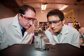 |
| UConn Assistant Professor Michael Pettes, left, and Ph.D. student Wei Wu check a device they created to exert strain on a semiconductor material only six atoms thick, on April 18, 2018. The project proved conclusively that the properties of atomically thin materials can be mechanically manipulated to enhance their performance. The findings could lead to faster computer processors and better optical sensors. CREDIT Peter Morenus/UConn Photo |
Abstract:
Researchers in UConn's Institute of Materials Science significantly improved the performance of an atomically thin semiconductor material by stretching it, an accomplishment that could prove beneficial to engineers designing the next generation of flexible electronics, nano devices, and optical sensors.
Strain improves performance of atomically thin semiconductor material
Storrs, CT | Posted on May 11th, 2018In a study appearing in the research journal Nano Letters, University of Connecticut Assistant Professor of Mechanical Engineering Michael Pettes reports that a six-atom thick bilayer of tungsten diselenide exhibited a 100-fold increase in photoluminescence when it was subjected to strain. The material had never exhibited such photoluminescence before.
The findings mark the first time scientists have been able to conclusively show that the properties of atomically thin materials can be mechanically manipulated to enhance their performance, Pettes says. Such capabilities could lead to faster computer processors and more efficient sensors.
The process the researchers used to achieve the outcome is also significant in that it offers a reliable new methodology for measuring the impact of strain on ultrathin materials, something that has been difficult to do and a hindrance to innovation.
"Experiments involving strain are often criticized since the strain experienced by these atomically thin materials is difficult to determine and often speculated as being incorrect," says Pettes. "Our study provides a new methodology for conducting strain-dependent measurements of ultrathin materials and this is important because strain is predicted to offer orders of magnitude changes in the properties of these materials across many different scientific fields."
Scientists have been intrigued by the potential of atomically thin materials ever since researchers Andre Geim and Konstantin Novoselov successfully cleaved a one-atom thick layer of graphene from a piece of graphite in 2004. Considered a supermaterial for its outstanding strength, flexibility, and ability to conduct electricity, two-dimensional graphene transformed the electronics industry and earned the researchers a Nobel Prize.
But for all that it offers, graphene has its limitations. It is a poor semiconductor because it lacks an electron band gap in its internal structure. As a result, electrons are unimpeded and flow rapidly through it when the material is energized. The best semiconductor materials, such as silicon, have a sizable band gap that allows a flow of electrons to be turned on and off. That capability is vital for creating the strings of zeros and ones that make up the binary computing codes used in transistors and integrated circuits.
Materials scientists are exploring the potential of other two-dimensional and atomically thin materials hoping to find products superior to graphene and silicon.
Strain engineering has been discussed as one possible way to enhance the performance of these materials because their ultrathin structure makes them particularly susceptible to bending and stretching, unlike their larger three-dimensional bulk forms. But testing the impact of strain on materials just a few atoms thick has proven enormously difficult.
In the present study, Pettes and Wei Wu, a Ph.D. student in Pettes' lab and the study's lead author, were able to successfully measure the influence of strain on a single crystalline bilayer of tungsten diselenide by first encapsulating it in a fine layer of acrylic glass and then heating it in an argon gas chamber. (Exposure to air would destroy the sample). This thermal processing strengthened the material's adhesion to a polymer substrate, allowing for a near perfect transfer of applied strain, which has been difficult to achieve in prior experiments.
The group then customized a bending device that allowed them to carefully increase strain on the material while monitoring how it responded through a Horiba Multiline Raman Spectrometer at the Harvard Center for Nanoscale Systems, a shared user facility funded by the National Science Foundation.
It was an exciting moment.
"Our new method allowed us to apply around two times more strain to the 2-D material than any previous study has reported," says Pettes. "Essentially, we were in new territory."
Ultimately, the researchers found that applying increasing levels of strain to the material altered its flow of electrons, which was reflected by the increased intensity in photoluminescence.
Working with UConn Assistant Professor of Materials Science and Engineering Avinash Dongare, an expert in computer modeling, and former Ph.D. student Jin Wang, the team was able to show that their process could, theoretically, manipulate the band gap of tungsten diselenide and other atomically thin materials, which is extremely important for design engineers seeking faster and more efficient semiconductors and sensors. Manipulating a semiconductor with an indirect band gap very near the point of transitioning to a direct band gap could lead to extremely fast processing capabilities.
"This is the first time that extrinsic control over an indirect-to-direct electron band gap transition has been conclusively reported," says Pettes. "Our findings should allow computational scientists using artificial intelligence to design new materials with extremely strain-resistant or strain-sensitive structures. That is extremely important for the next generation of high performance flexible nanoelectronics and optoelectronic devices."
Joining Pettes and Wu on the research were two undergraduate students: UConn senior Nico Wright, a former McNair Scholar and participant in NSF's Research Experiences for Undergraduates (REU) program; and Danielle Leppert-Simenauer, also a former participant in NSF's REU program and currently an undergraduate majoring in physics at the University of California-San Diego.
The U.S. Army Research Laboratory in Adelphi, Maryland provided graphene films that were used to confirm the calibration standards applied by the UConn researchers to measure strain. The atomic-level thickness of the tungsten diselenide bilayer was confirmed through transmission electron microscopy in the Molecular Foundry at Lawrence Berkeley National Laboratory.
####
For more information, please click here
Contacts:
Colin Poitras
860-486-4656
Copyright © University of Connecticut
If you have a comment, please Contact us.Issuers of news releases, not 7th Wave, Inc. or Nanotechnology Now, are solely responsible for the accuracy of the content.
Bookmark:


| Related Links |
| Related News Press |
News and information
![]() Quantum computer improves AI predictions April 17th, 2026
Quantum computer improves AI predictions April 17th, 2026
![]() Flexible sensor gains sensitivity under pressure April 17th, 2026
Flexible sensor gains sensitivity under pressure April 17th, 2026
![]() A reusable chip for particulate matter sensing April 17th, 2026
A reusable chip for particulate matter sensing April 17th, 2026
![]() Detecting vibrational quantum beating in the predissociation dynamics of SF6 using time-resolved photoelectron spectroscopy April 17th, 2026
Detecting vibrational quantum beating in the predissociation dynamics of SF6 using time-resolved photoelectron spectroscopy April 17th, 2026
Flexible Electronics
![]() Flexible sensor gains sensitivity under pressure April 17th, 2026
Flexible sensor gains sensitivity under pressure April 17th, 2026
2 Dimensional Materials
![]() Flexible sensor gains sensitivity under pressure April 17th, 2026
Flexible sensor gains sensitivity under pressure April 17th, 2026
Graphene/ Graphite
![]() Electrifying results shed light on graphene foam as a potential material for lab grown cartilage June 6th, 2025
Electrifying results shed light on graphene foam as a potential material for lab grown cartilage June 6th, 2025
Nanofabrication
![]() Self-propelled protein-based nanomotors for enhanced cancer therapy by inducing ferroptosis June 6th, 2025
Self-propelled protein-based nanomotors for enhanced cancer therapy by inducing ferroptosis June 6th, 2025
![]() Multiphoton polymerization: A promising technology for precision medicine February 28th, 2025
Multiphoton polymerization: A promising technology for precision medicine February 28th, 2025
Hardware
![]() The present and future of computing get a boost from new research July 21st, 2023
The present and future of computing get a boost from new research July 21st, 2023
![]() A Carbon Nanotube Microprocessor Mature Enough to Say Hello: Three new breakthroughs make commercial nanotube processors possible March 2nd, 2020
A Carbon Nanotube Microprocessor Mature Enough to Say Hello: Three new breakthroughs make commercial nanotube processors possible March 2nd, 2020
![]() Powering the future: Smallest all-digital circuit opens doors to 5 nm next-gen semiconductor February 11th, 2020
Powering the future: Smallest all-digital circuit opens doors to 5 nm next-gen semiconductor February 11th, 2020
Govt.-Legislation/Regulation/Funding/Policy
![]() Quantum computer improves AI predictions April 17th, 2026
Quantum computer improves AI predictions April 17th, 2026
![]() Metasurfaces smooth light to boost magnetic sensing precision January 30th, 2026
Metasurfaces smooth light to boost magnetic sensing precision January 30th, 2026
![]() New imaging approach transforms study of bacterial biofilms August 8th, 2025
New imaging approach transforms study of bacterial biofilms August 8th, 2025
Possible Futures
![]() A fundamentally new therapeutic approach to cystic fibrosis: Nanobody repairs cellular defect April 17th, 2026
A fundamentally new therapeutic approach to cystic fibrosis: Nanobody repairs cellular defect April 17th, 2026
![]() UC Irvine physicists discover method to reverse �quantum scrambling� : The work addresses the problem of information loss in quantum computing system April 17th, 2026
UC Irvine physicists discover method to reverse �quantum scrambling� : The work addresses the problem of information loss in quantum computing system April 17th, 2026
Chip Technology
![]() A reusable chip for particulate matter sensing April 17th, 2026
A reusable chip for particulate matter sensing April 17th, 2026
![]() Metasurfaces smooth light to boost magnetic sensing precision January 30th, 2026
Metasurfaces smooth light to boost magnetic sensing precision January 30th, 2026
Optical computing/Photonic computing
![]() ICFO researchers overcome long-standing bottleneck in single photon detection with twisted 2D materials August 8th, 2025
ICFO researchers overcome long-standing bottleneck in single photon detection with twisted 2D materials August 8th, 2025
![]() Programmable electron-induced color router array May 14th, 2025
Programmable electron-induced color router array May 14th, 2025
Sensors
![]() Flexible sensor gains sensitivity under pressure April 17th, 2026
Flexible sensor gains sensitivity under pressure April 17th, 2026
![]() Tiny nanosheets, big leap: A new sensor detects ethanol at ultra-low levels January 30th, 2026
Tiny nanosheets, big leap: A new sensor detects ethanol at ultra-low levels January 30th, 2026
![]() From sensors to smart systems: the rise of AI-driven photonic noses January 30th, 2026
From sensors to smart systems: the rise of AI-driven photonic noses January 30th, 2026
![]() Sensors innovations for smart lithium-based batteries: advancements, opportunities, and potential challenges August 8th, 2025
Sensors innovations for smart lithium-based batteries: advancements, opportunities, and potential challenges August 8th, 2025
Nanoelectronics
![]() Lab to industry: InSe wafer-scale breakthrough for future electronics August 8th, 2025
Lab to industry: InSe wafer-scale breakthrough for future electronics August 8th, 2025
![]() Interdisciplinary: Rice team tackles the future of semiconductors Multiferroics could be the key to ultralow-energy computing October 6th, 2023
Interdisciplinary: Rice team tackles the future of semiconductors Multiferroics could be the key to ultralow-energy computing October 6th, 2023
![]() Key element for a scalable quantum computer: Physicists from Forschungszentrum J�lich and RWTH Aachen University demonstrate electron transport on a quantum chip September 23rd, 2022
Key element for a scalable quantum computer: Physicists from Forschungszentrum J�lich and RWTH Aachen University demonstrate electron transport on a quantum chip September 23rd, 2022
![]() Reduced power consumption in semiconductor devices September 23rd, 2022
Reduced power consumption in semiconductor devices September 23rd, 2022
Discoveries
![]() Quantum computer improves AI predictions April 17th, 2026
Quantum computer improves AI predictions April 17th, 2026
![]() Flexible sensor gains sensitivity under pressure April 17th, 2026
Flexible sensor gains sensitivity under pressure April 17th, 2026
![]() A reusable chip for particulate matter sensing April 17th, 2026
A reusable chip for particulate matter sensing April 17th, 2026
![]() Detecting vibrational quantum beating in the predissociation dynamics of SF6 using time-resolved photoelectron spectroscopy April 17th, 2026
Detecting vibrational quantum beating in the predissociation dynamics of SF6 using time-resolved photoelectron spectroscopy April 17th, 2026
Announcements
![]() A fundamentally new therapeutic approach to cystic fibrosis: Nanobody repairs cellular defect April 17th, 2026
A fundamentally new therapeutic approach to cystic fibrosis: Nanobody repairs cellular defect April 17th, 2026
![]() UC Irvine physicists discover method to reverse �quantum scrambling� : The work addresses the problem of information loss in quantum computing system April 17th, 2026
UC Irvine physicists discover method to reverse �quantum scrambling� : The work addresses the problem of information loss in quantum computing system April 17th, 2026
Interviews/Book Reviews/Essays/Reports/Podcasts/Journals/White papers/Posters
![]() A fundamentally new therapeutic approach to cystic fibrosis: Nanobody repairs cellular defect April 17th, 2026
A fundamentally new therapeutic approach to cystic fibrosis: Nanobody repairs cellular defect April 17th, 2026
![]() UC Irvine physicists discover method to reverse �quantum scrambling� : The work addresses the problem of information loss in quantum computing system April 17th, 2026
UC Irvine physicists discover method to reverse �quantum scrambling� : The work addresses the problem of information loss in quantum computing system April 17th, 2026
Artificial Intelligence
![]() Quantum computer improves AI predictions April 17th, 2026
Quantum computer improves AI predictions April 17th, 2026
![]() From sensors to smart systems: the rise of AI-driven photonic noses January 30th, 2026
From sensors to smart systems: the rise of AI-driven photonic noses January 30th, 2026
![]() New quantum encoding methods slash circuit complexity in machine learning November 8th, 2024
New quantum encoding methods slash circuit complexity in machine learning November 8th, 2024
Photonics/Optics/Lasers
![]() Metasurfaces smooth light to boost magnetic sensing precision January 30th, 2026
Metasurfaces smooth light to boost magnetic sensing precision January 30th, 2026
![]() From sensors to smart systems: the rise of AI-driven photonic noses January 30th, 2026
From sensors to smart systems: the rise of AI-driven photonic noses January 30th, 2026
|
|
||
|
|
||
| The latest news from around the world, FREE | ||
|
|
||
|
|
||
| Premium Products | ||
|
|
||
|
Only the news you want to read!
Learn More |
||
|
|
||
|
Full-service, expert consulting
Learn More |
||
|
|
||