Home > Press > RIT researchers improve fabrication process of nano-structures for electronic devices: Use of indium gallium phosphide with I-MacEtch processing shows promise for more cost effective fabrication and increased performance in devices from photonics to telecommunications
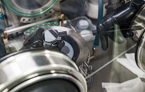 |
| University Web Services Semiconductor devices are created on wafers through a multi-step process to coat, remove or pattern conductive materials. |
Abstract:
Researchers at RIT have found a more efficient fabricating process to produce semiconductors used in today’s electronic devices. They also confirmed that materials other than silicon can be used successfully in the development process that could increase performance of electronic devices. This fabrication process—the I-MacEtch, or inverse metal-assisted chemical etching method—can help meet the growing demand for more powerful and reliable nano-technologies needed for solar cells, smartphones, telecommunications grids and new applications in photonics and quantum computing.
RIT researchers improve fabrication process of nano-structures for electronic devices: Use of indium gallium phosphide with I-MacEtch processing shows promise for more cost effective fabrication and increased performance in devices from photonics to telecommunications
Rochester, NY | Posted on March 20th, 2018“What is novel about our work is that for the first time we are looking at applying I-MacEtch processing to indium-gallium-phosphide materials. I-MacEtch is an alternative to two conventional approaches and is a technique that has been used in the field—but the materials that have been explored are fairly limited,” said Parsian Mohseni, assistant professor of microsystems engineering in RIT’s Kate Gleason College of Engineering. He is also director of the EINS Laboratory at the university.
Demands for improved computer processing power have led researchers to explore both new processes and other materials beyond silicon to produce electronic components, Mohseni explained. The I-MacEtch process combines the benefits of two traditional methods—wet etching and reactive ion etching, or REI. Indium-gallium-phosphide is one of several materials being tested to complement silicon as a means to improve current capacity of semiconductor processing.
“This is a very well-known material and has applications in the electronics and solar cell industries,” he said. “We are not re-inventing the wheel; we are establishing new protocols for treating the existing material that is more cost effective, and a more sustainable process.”
Semiconductor devices are created on wafers through a multi-step process to coat, remove or pattern conductive materials. Traditional processes are wet etch, where a sample with blocked aspects is immersed in an acid bath to remove substances, and reactive ion etching, where ions bombard exposed surfaces on the wafer to change its chemical properties and remove materials in those exposed regions. Both have been used to develop the intricate electronic patterns on circuits and use silicon as a foundation for this type of patterning. Improving patterning methods by I-MacEtch could mean reducing fabrication complexity of various photonic and electronic devices.
Researchers and semiconductor fabrication scientists have been using MacEtch extensively for processing silicon. At the same time, assessments of other materials in the III-V range of individual elements that may be conducive to this same type of fabrication with similar advantages are underway. In his research, Mohseni is also looking at different alloys of those III-V materials, namely the ternary alloys such as indium-gallium-phosphide (InGaP).
The research detailed in the upcoming issue of the American Chemical Society’s Applied Materials and Interfaces journal highlights how the nanofabrication methodology was applied to InGaP and how it can impact the processing of device applications and generation of high aspect ratio and nano-scale semiconductor features, said Thomas Wilhelm, a microsystems engineering doctoral student and first-author of the paper. The novel processing method can be significant in the development of ordered arrays of high aspect ratio structures such as nanowires.
For solar cells, the goal is to minimize the cost-to-power-produced ratio, and if it is possible to lower the cost of making the cell, and increasing the efficiency of it, this improves the device overall. Exploring new methods of fabricating the existing, relevant materials in a way that allows for faster, less expensive and more controlled processing by combining the benefits of wet etching and RIE has been the focus of Mohseni’s work. The improved process means avoiding expensive, bulky, hazardous processing methods.
“We are using a simple benchtop set up and we end up with very similar structures; in fact, one can argue that they are higher in quality than the structures that we can generate with RIE for a fraction of the cost and with less time, less steps throughout, without the higher temperature conditions or expensive instrumentation,” he said.
####
About Rochester Institute of Technology
Rochester Institute of Technology is home to leading creators, entrepreneurs, innovators and researchers. Founded in 1829, RIT enrolls about 19,000 students in more than 200 career-oriented and professional programs, making it among the largest private universities in the U.S.
The university is internationally recognized and ranked for academic leadership in business, computing, engineering, imaging science, liberal arts, sustainability, and fine and applied arts. RIT also offers unparalleled support services for deaf and hard-of-hearing students. The cooperative education program is one of the oldest and largest in the nation. Global partnerships include campuses in China, Croatia, Dubai and Kosovo.
For news, photos and videos, go to www.rit.edu/news.
For more information, please click here
Contacts:
Michelle Cometa
585-475-4954
Copyright © Rochester Institute of Technology
If you have a comment, please Contact us.Issuers of news releases, not 7th Wave, Inc. or Nanotechnology Now, are solely responsible for the accuracy of the content.
Bookmark:


| Related News Press |
News and information
![]() Quantum computer improves AI predictions April 17th, 2026
Quantum computer improves AI predictions April 17th, 2026
![]() Flexible sensor gains sensitivity under pressure April 17th, 2026
Flexible sensor gains sensitivity under pressure April 17th, 2026
![]() A reusable chip for particulate matter sensing April 17th, 2026
A reusable chip for particulate matter sensing April 17th, 2026
![]() Detecting vibrational quantum beating in the predissociation dynamics of SF6 using time-resolved photoelectron spectroscopy April 17th, 2026
Detecting vibrational quantum beating in the predissociation dynamics of SF6 using time-resolved photoelectron spectroscopy April 17th, 2026
Wireless/telecommunications/RF/Antennas/Microwaves
![]() Researchers develop molecular qubits that communicate at telecom frequencies October 3rd, 2025
Researchers develop molecular qubits that communicate at telecom frequencies October 3rd, 2025
Nanofabrication
![]() Self-propelled protein-based nanomotors for enhanced cancer therapy by inducing ferroptosis June 6th, 2025
Self-propelled protein-based nanomotors for enhanced cancer therapy by inducing ferroptosis June 6th, 2025
![]() Multiphoton polymerization: A promising technology for precision medicine February 28th, 2025
Multiphoton polymerization: A promising technology for precision medicine February 28th, 2025
![]() New chip opens door to AI computing at light speed February 16th, 2024
New chip opens door to AI computing at light speed February 16th, 2024
Possible Futures
![]() A fundamentally new therapeutic approach to cystic fibrosis: Nanobody repairs cellular defect April 17th, 2026
A fundamentally new therapeutic approach to cystic fibrosis: Nanobody repairs cellular defect April 17th, 2026
![]() UC Irvine physicists discover method to reverse ‘quantum scrambling’ : The work addresses the problem of information loss in quantum computing system April 17th, 2026
UC Irvine physicists discover method to reverse ‘quantum scrambling’ : The work addresses the problem of information loss in quantum computing system April 17th, 2026
Chip Technology
![]() A reusable chip for particulate matter sensing April 17th, 2026
A reusable chip for particulate matter sensing April 17th, 2026
![]() Metasurfaces smooth light to boost magnetic sensing precision January 30th, 2026
Metasurfaces smooth light to boost magnetic sensing precision January 30th, 2026
Quantum Computing
![]() Quantum computer improves AI predictions April 17th, 2026
Quantum computer improves AI predictions April 17th, 2026
![]() UC Irvine physicists discover method to reverse ‘quantum scrambling’ : The work addresses the problem of information loss in quantum computing system April 17th, 2026
UC Irvine physicists discover method to reverse ‘quantum scrambling’ : The work addresses the problem of information loss in quantum computing system April 17th, 2026
![]() Researchers develop molecular qubits that communicate at telecom frequencies October 3rd, 2025
Researchers develop molecular qubits that communicate at telecom frequencies October 3rd, 2025
Optical computing/Photonic computing
![]() ICFO researchers overcome long-standing bottleneck in single photon detection with twisted 2D materials August 8th, 2025
ICFO researchers overcome long-standing bottleneck in single photon detection with twisted 2D materials August 8th, 2025
![]() Programmable electron-induced color router array May 14th, 2025
Programmable electron-induced color router array May 14th, 2025
Nanoelectronics
![]() Lab to industry: InSe wafer-scale breakthrough for future electronics August 8th, 2025
Lab to industry: InSe wafer-scale breakthrough for future electronics August 8th, 2025
![]() Interdisciplinary: Rice team tackles the future of semiconductors Multiferroics could be the key to ultralow-energy computing October 6th, 2023
Interdisciplinary: Rice team tackles the future of semiconductors Multiferroics could be the key to ultralow-energy computing October 6th, 2023
![]() Key element for a scalable quantum computer: Physicists from Forschungszentrum Jülich and RWTH Aachen University demonstrate electron transport on a quantum chip September 23rd, 2022
Key element for a scalable quantum computer: Physicists from Forschungszentrum Jülich and RWTH Aachen University demonstrate electron transport on a quantum chip September 23rd, 2022
![]() Reduced power consumption in semiconductor devices September 23rd, 2022
Reduced power consumption in semiconductor devices September 23rd, 2022
Discoveries
![]() Quantum computer improves AI predictions April 17th, 2026
Quantum computer improves AI predictions April 17th, 2026
![]() Flexible sensor gains sensitivity under pressure April 17th, 2026
Flexible sensor gains sensitivity under pressure April 17th, 2026
![]() A reusable chip for particulate matter sensing April 17th, 2026
A reusable chip for particulate matter sensing April 17th, 2026
![]() Detecting vibrational quantum beating in the predissociation dynamics of SF6 using time-resolved photoelectron spectroscopy April 17th, 2026
Detecting vibrational quantum beating in the predissociation dynamics of SF6 using time-resolved photoelectron spectroscopy April 17th, 2026
Announcements
![]() A fundamentally new therapeutic approach to cystic fibrosis: Nanobody repairs cellular defect April 17th, 2026
A fundamentally new therapeutic approach to cystic fibrosis: Nanobody repairs cellular defect April 17th, 2026
![]() UC Irvine physicists discover method to reverse ‘quantum scrambling’ : The work addresses the problem of information loss in quantum computing system April 17th, 2026
UC Irvine physicists discover method to reverse ‘quantum scrambling’ : The work addresses the problem of information loss in quantum computing system April 17th, 2026
Interviews/Book Reviews/Essays/Reports/Podcasts/Journals/White papers/Posters
![]() A fundamentally new therapeutic approach to cystic fibrosis: Nanobody repairs cellular defect April 17th, 2026
A fundamentally new therapeutic approach to cystic fibrosis: Nanobody repairs cellular defect April 17th, 2026
![]() UC Irvine physicists discover method to reverse ‘quantum scrambling’ : The work addresses the problem of information loss in quantum computing system April 17th, 2026
UC Irvine physicists discover method to reverse ‘quantum scrambling’ : The work addresses the problem of information loss in quantum computing system April 17th, 2026
Energy
![]() Sensors innovations for smart lithium-based batteries: advancements, opportunities, and potential challenges August 8th, 2025
Sensors innovations for smart lithium-based batteries: advancements, opportunities, and potential challenges August 8th, 2025
![]() Simple algorithm paired with standard imaging tool could predict failure in lithium metal batteries August 8th, 2025
Simple algorithm paired with standard imaging tool could predict failure in lithium metal batteries August 8th, 2025
Photonics/Optics/Lasers
![]() Metasurfaces smooth light to boost magnetic sensing precision January 30th, 2026
Metasurfaces smooth light to boost magnetic sensing precision January 30th, 2026
![]() From sensors to smart systems: the rise of AI-driven photonic noses January 30th, 2026
From sensors to smart systems: the rise of AI-driven photonic noses January 30th, 2026
Solar/Photovoltaic
![]() Spinel-type sulfide semiconductors to operate the next-generation LEDs and solar cells For solar-cell absorbers and green-LED source October 3rd, 2025
Spinel-type sulfide semiconductors to operate the next-generation LEDs and solar cells For solar-cell absorbers and green-LED source October 3rd, 2025
![]() KAIST researchers introduce new and improved, next-generation perovskite solar cell November 8th, 2024
KAIST researchers introduce new and improved, next-generation perovskite solar cell November 8th, 2024
![]() Groundbreaking precision in single-molecule optoelectronics August 16th, 2024
Groundbreaking precision in single-molecule optoelectronics August 16th, 2024
![]() Development of zinc oxide nanopagoda array photoelectrode: photoelectrochemical water-splitting hydrogen production January 12th, 2024
Development of zinc oxide nanopagoda array photoelectrode: photoelectrochemical water-splitting hydrogen production January 12th, 2024
|
|
||
|
|
||
| The latest news from around the world, FREE | ||
|
|
||
|
|
||
| Premium Products | ||
|
|
||
|
Only the news you want to read!
Learn More |
||
|
|
||
|
Full-service, expert consulting
Learn More |
||
|
|
||