Home > Press > Tungsten offers nano-interconnects a path of least resistance: Crystalline tungsten shows insight and promise in addressing the challenges of electrical interconnects that have high resistivity at the nanoscale
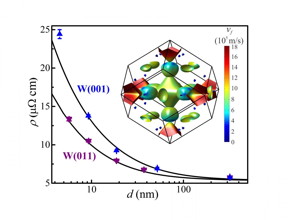 |
| The measured resistivity of epitaxial tungsten layers with (001) and (011) crystal orientation vs thickness d. The tungsten Fermi surface is color coded according to the wave vector dependent Fermi velocity vf. At small thickness, where surface scattering dominates, W(011) is nearly twice as conductive as W(001). Transport simulations indicate that this is due to the anisotropy in the Fermi surface. These results indicate how narrow wires in future computer chips can be made two times more conductive, effectively reducing the required electric power by 50 percent. CREDIT Daniel Gall, Rensselaer Polytechnic Institute |
Abstract:
As microchips become ever smaller and therefore faster, the shrinking size of their copper interconnects leads to increased electrical resistivity at the nanoscale. Finding a solution to this impending technical bottleneck is a major problem for the semiconductor industry.
Tungsten offers nano-interconnects a path of least resistance: Crystalline tungsten shows insight and promise in addressing the challenges of electrical interconnects that have high resistivity at the nanoscale
Washington, DC | Posted on October 4th, 2017One promising possibility involves reducing the resistivity size effect by altering the crystalline orientation of interconnect materials. A pair of researchers from Rensselaer Polytechnic Institute conducted electron transport measurements in epitaxial single-crystal layers of tungsten (W) as one such potential interconnect solution. They performed first-principles simulations, finding a definite orientation-dependent effect. The anisotropic resistivity effect they found was most marked between layers with two particular orientations of the lattice structure, namely W(001) and W(110). The work is published this week in the Journal of Applied Physics, from AIP Publishing.
Author Pengyuan Zheng noted that both the 2013 and 2015 International Technology Roadmap for Semiconductors (ITRS) called for new materials to replace copper as interconnect material to limit resistance increase at reduced scale and minimize both power consumption and signal delay.
In their study, Zheng and co-author Daniel Gall chose tungsten because of its asymmetric Fermi surface -- its electron energy structure. This made it a good candidate to demonstrate the anisotropic resistivity effect at the small scales of interest. "The bulk material is completely isotropic, so the resistivity is the same in all directions," Gall said. "But if we have thin films, then the resistivity varies considerably."
To test the most promising orientations, the researchers grew epitaxial W(001) and W(110) films on substrates and conducted resistivity measurements of both while immersed in liquid nitrogen at 77 Kelvin (about -196 degrees Celsius) and at room temperature, or 295 Kelvin. "We had roughly a factor of 2 difference in the resistivity between the 001 oriented tungsten and 110 oriented tungsten," Gall said, but they found considerably smaller resistivity in the W(011) layers.
Although the measured anisotropic resistance effect was in good agreement with what they expected from calculations, the effective mean free path -- the average distance electrons can move before scattering against a boundary -- in the thin film experiments was much larger than the theoretical value for bulk tungsten.
"An electron travels through a wire on a diagonal, it hits a surface, gets scattered, and then continues traveling until it hits something else, maybe the other side of the wire or a lattice vibration," Gall said. "But this model looks wrong for small wires."
The experimenters believe this may be explained by quantum mechanical processes of the electrons that arise at these limited scales. Electrons may be simultaneously touching both sides of the wire or experiencing increased electron-phonon (lattice vibrations) coupling as the layer thickness decreases, phenomena that could affect the search for another metal to replace copper interconnects.
"The envisioned conductivity advantages of rhodium, iridium, and nickel may be smaller than predicted," said Zheng. Findings like these will prove increasingly important as quantum mechanical scales become more commonplace for the demands of interconnects.
The research team is continuing to explore the anisotropic size effect in other metals with nonspherical Fermi surfaces, such as molybdenum. They found that the orientation of the surface relative to the layer orientation and transport direction is vital, as it determines the actual increase in resistivity at these reduced dimensions.
"The results presented in this paper clearly demonstrate that the correct choice of crystalline orientation has the potential to reduce nanowire resistance," said Zheng. The importance of the work extends beyond current nanoelectronics to new and developing technologies, including transparent flexible conductors, thermoelectrics and memristors that can potentially store information. "It's the problem that defines what you can do in the next technology," Gall said.
####
About American Institute of Physics
Journal of Applied Physics features full length reports on significant new findings in applied physics. The journal covers new experimental and theoretical research on applications of physics phenomena related to all branches of science, engineering, and modern technology. See http://jap.aip.org .
For more information, please click here
Contacts:
Julia Majors
301-209-3090
Copyright © American Institute of Physics
If you have a comment, please Contact us.Issuers of news releases, not 7th Wave, Inc. or Nanotechnology Now, are solely responsible for the accuracy of the content.
Bookmark:


| Related Links |
| Related News Press |
News and information
![]() Quantum computer improves AI predictions April 17th, 2026
Quantum computer improves AI predictions April 17th, 2026
![]() Flexible sensor gains sensitivity under pressure April 17th, 2026
Flexible sensor gains sensitivity under pressure April 17th, 2026
![]() A reusable chip for particulate matter sensing April 17th, 2026
A reusable chip for particulate matter sensing April 17th, 2026
![]() Detecting vibrational quantum beating in the predissociation dynamics of SF6 using time-resolved photoelectron spectroscopy April 17th, 2026
Detecting vibrational quantum beating in the predissociation dynamics of SF6 using time-resolved photoelectron spectroscopy April 17th, 2026
Flexible Electronics
![]() Flexible sensor gains sensitivity under pressure April 17th, 2026
Flexible sensor gains sensitivity under pressure April 17th, 2026
![]() MXene nanomaterials enter a new dimension Multilayer nanomaterial: MXene flakes created at Drexel University show new promise as 1D scrolls January 30th, 2026
MXene nanomaterials enter a new dimension Multilayer nanomaterial: MXene flakes created at Drexel University show new promise as 1D scrolls January 30th, 2026
Physics
![]() UC Irvine physicists discover method to reverse �quantum scrambling� : The work addresses the problem of information loss in quantum computing system April 17th, 2026
UC Irvine physicists discover method to reverse �quantum scrambling� : The work addresses the problem of information loss in quantum computing system April 17th, 2026
Hardware
![]() The present and future of computing get a boost from new research July 21st, 2023
The present and future of computing get a boost from new research July 21st, 2023
![]() A Carbon Nanotube Microprocessor Mature Enough to Say Hello: Three new breakthroughs make commercial nanotube processors possible March 2nd, 2020
A Carbon Nanotube Microprocessor Mature Enough to Say Hello: Three new breakthroughs make commercial nanotube processors possible March 2nd, 2020
![]() Powering the future: Smallest all-digital circuit opens doors to 5 nm next-gen semiconductor February 11th, 2020
Powering the future: Smallest all-digital circuit opens doors to 5 nm next-gen semiconductor February 11th, 2020
Possible Futures
![]() A fundamentally new therapeutic approach to cystic fibrosis: Nanobody repairs cellular defect April 17th, 2026
A fundamentally new therapeutic approach to cystic fibrosis: Nanobody repairs cellular defect April 17th, 2026
![]() UC Irvine physicists discover method to reverse �quantum scrambling� : The work addresses the problem of information loss in quantum computing system April 17th, 2026
UC Irvine physicists discover method to reverse �quantum scrambling� : The work addresses the problem of information loss in quantum computing system April 17th, 2026
Chip Technology
![]() A reusable chip for particulate matter sensing April 17th, 2026
A reusable chip for particulate matter sensing April 17th, 2026
![]() Metasurfaces smooth light to boost magnetic sensing precision January 30th, 2026
Metasurfaces smooth light to boost magnetic sensing precision January 30th, 2026
Nanoelectronics
![]() Lab to industry: InSe wafer-scale breakthrough for future electronics August 8th, 2025
Lab to industry: InSe wafer-scale breakthrough for future electronics August 8th, 2025
![]() Interdisciplinary: Rice team tackles the future of semiconductors Multiferroics could be the key to ultralow-energy computing October 6th, 2023
Interdisciplinary: Rice team tackles the future of semiconductors Multiferroics could be the key to ultralow-energy computing October 6th, 2023
![]() Key element for a scalable quantum computer: Physicists from Forschungszentrum J�lich and RWTH Aachen University demonstrate electron transport on a quantum chip September 23rd, 2022
Key element for a scalable quantum computer: Physicists from Forschungszentrum J�lich and RWTH Aachen University demonstrate electron transport on a quantum chip September 23rd, 2022
![]() Reduced power consumption in semiconductor devices September 23rd, 2022
Reduced power consumption in semiconductor devices September 23rd, 2022
Discoveries
![]() Quantum computer improves AI predictions April 17th, 2026
Quantum computer improves AI predictions April 17th, 2026
![]() Flexible sensor gains sensitivity under pressure April 17th, 2026
Flexible sensor gains sensitivity under pressure April 17th, 2026
![]() A reusable chip for particulate matter sensing April 17th, 2026
A reusable chip for particulate matter sensing April 17th, 2026
![]() Detecting vibrational quantum beating in the predissociation dynamics of SF6 using time-resolved photoelectron spectroscopy April 17th, 2026
Detecting vibrational quantum beating in the predissociation dynamics of SF6 using time-resolved photoelectron spectroscopy April 17th, 2026
Announcements
![]() A fundamentally new therapeutic approach to cystic fibrosis: Nanobody repairs cellular defect April 17th, 2026
A fundamentally new therapeutic approach to cystic fibrosis: Nanobody repairs cellular defect April 17th, 2026
![]() UC Irvine physicists discover method to reverse �quantum scrambling� : The work addresses the problem of information loss in quantum computing system April 17th, 2026
UC Irvine physicists discover method to reverse �quantum scrambling� : The work addresses the problem of information loss in quantum computing system April 17th, 2026
Interviews/Book Reviews/Essays/Reports/Podcasts/Journals/White papers/Posters
![]() A fundamentally new therapeutic approach to cystic fibrosis: Nanobody repairs cellular defect April 17th, 2026
A fundamentally new therapeutic approach to cystic fibrosis: Nanobody repairs cellular defect April 17th, 2026
![]() UC Irvine physicists discover method to reverse �quantum scrambling� : The work addresses the problem of information loss in quantum computing system April 17th, 2026
UC Irvine physicists discover method to reverse �quantum scrambling� : The work addresses the problem of information loss in quantum computing system April 17th, 2026
|
|
||
|
|
||
| The latest news from around the world, FREE | ||
|
|
||
|
|
||
| Premium Products | ||
|
|
||
|
Only the news you want to read!
Learn More |
||
|
|
||
|
Full-service, expert consulting
Learn More |
||
|
|
||