Home > Press > Electron highway inside crystal
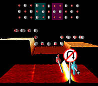 |
| Step edges on topological crystalline insulators may lead to electrically conducting pathways where electrons with opposite spin spin move in converse directions -- any U-turn is prohibited. Picture: Thomas Bathon/Paolo Sessi/Matthias Bode |
Abstract:
Physicists of the University of Würzburg have made an astonishing discovery in a specific type of topological insulators. The effect is due to the structure of the materials used. The researchers have now published their work in the journal Science.
Electron highway inside crystal
Würzburg, Germany | Posted on December 12th, 2016Topological insulators are currently the hot topic in physics according to the newspaper Neue Zürcher Zeitung. Only a few weeks ago, their importance was highlighted again as the Royal Swedish Academy of Sciences in Stockholm awarded this year's Nobel Prize in Physics to three British scientists for their research of so-called topological phase transitions and topological phases of matter.
Topological insulators are also being studied at the Departments for Experimental Physics II and Theoretical Physics I of the University of Würzburg. However, they focus on a special version of insulators called topological crystalline insulators (TCI). In cooperation with the Polish Academy of Sciences in Warsaw and the University of Zurich, Würzburg physicists have now achieved a major breakthrough. They were able to detect new electronic states of matter in these insulators. The results of their work are published in the latest issue of Science.
Step edges direct electrons
The central result: When crystalline materials are split, small atomically flat terraces emerge at the split off surfaces which are separated from each other by step edges. Inside these structures, conductive channels for electrical currents form which are extremely narrow at just about 10 nm and surprisingly robust against external disturbance. Electrons travel on these conductive channels with different spin in opposite directions - similar to a motorway with separate lanes for the two directions. This effect makes the materials interesting for technological applications in future electronic components such as ultra-fast and energy-efficient computers.
"TCIs are relatively simple to produce and they are already different from conventional materials because of their special crystalline structure," Dr. Paolo Sessi explains the background of the recently published paper. Sessi is a research fellow at the Department of Experimental Physics II and the lead author of the study. Moreover, these materials owe their special quality to their electronic properties: In topological materials, the direction of spin determines the direction in which the electrons travel. Simply put, the "spin" can be interpreted as a magnetic dipole that can point in two directions ("up" and "down"). Accordingly, up-spin electrons in TCIs move in one and down-spin electrons in the other direction.
It's all about the number of atomic layers
"But previously scientists didn't know how to produce the conductive channels required to this end," says Professor Matthias Bode, Head of the Department for Experimental Physics II and co-author of the study. It was chance that now got the researchers on the right track: They discovered that very narrow conductive channels occur naturally when splitting lead tin selenide (PbSnSe), a crystalline insulator.
Step edges on the fragments' surfaces cause this phenomenon. They can be imaged using a high-resolution scanning tunnelling microscopy, or more precisely, the height of the corresponding step edges. "Edges that bridge an even number of atomic layers are totally inconspicuous. But if the edges span an odd number of atomic layers, a small area about 10 nm in width is created that has the electronic conductive channels properties we were looking for," Sessi explains.
Pattern breaks off at the edge
Supported by their colleagues from the Department of Theoretical Physics I and the University of Zurich, the experimental physicists were able to shed light on the origin of these new electronic states. To understand the principle, a little spatial sense is required:
"The crystalline structure causes a layout of the atoms where the different elements alternate like the black and white squares on a chessboard," Matthias Bode explains. This alternating black-and-white pattern applies to both squares which are adjacent and squares situated below and on top one another.
So if the crack of this crystal runs through different atomic layers, more than one edge is created there. Seen from above, white squares may also abut to other white squares along this edge and black squares to other black squares - or identical atoms to identical atoms. However, this only works if an odd number of atomic layers is responsible for the difference in height of the two surfaces.
Backed by calculations
"Calculations show that this offset at the surface is actually causative of these novel electronic states," says Paolo Sessi. Furthermore, they prove that the phenomenon of the spin-dependent conductive channels, which is characteristic of topological materials, occurs here as well.
According to the scientists, this property in particular makes the discovery relevant for potential applications, because such conductive channels cause low conduction loss on the one hand and can be used directly to transmit and process information in the field of spintronics on the other.
However, several questions need to be answered and challenges to be overcome before this will become reality. For instance, the scientists are not yet sure over which distances the currents in the newly discovered conductive channels can be transported. Also, in order to be implemented in circuits, methods would have to be developed that allow creating step edges of a defined height along specified directions.
####
For more information, please click here
Contacts:
Dr. Paolo Sessi
49-931-318-8021
Copyright © University of Würzburg
If you have a comment, please Contact us.Issuers of news releases, not 7th Wave, Inc. or Nanotechnology Now, are solely responsible for the accuracy of the content.
Bookmark:


| Related Links |
| Related News Press |
News and information
![]() Quantum computer improves AI predictions April 17th, 2026
Quantum computer improves AI predictions April 17th, 2026
![]() Flexible sensor gains sensitivity under pressure April 17th, 2026
Flexible sensor gains sensitivity under pressure April 17th, 2026
![]() A reusable chip for particulate matter sensing April 17th, 2026
A reusable chip for particulate matter sensing April 17th, 2026
![]() Detecting vibrational quantum beating in the predissociation dynamics of SF6 using time-resolved photoelectron spectroscopy April 17th, 2026
Detecting vibrational quantum beating in the predissociation dynamics of SF6 using time-resolved photoelectron spectroscopy April 17th, 2026
Videos/Movies
![]() ICFO researchers overcome long-standing bottleneck in single photon detection with twisted 2D materials August 8th, 2025
ICFO researchers overcome long-standing bottleneck in single photon detection with twisted 2D materials August 8th, 2025
![]() New X-ray imaging technique to study the transient phases of quantum materials December 29th, 2022
New X-ray imaging technique to study the transient phases of quantum materials December 29th, 2022
![]() Solvent study solves solar cell durability puzzle: Rice-led project could make perovskite cells ready for prime time September 23rd, 2022
Solvent study solves solar cell durability puzzle: Rice-led project could make perovskite cells ready for prime time September 23rd, 2022
![]() Scientists prepare for the world’s smallest race: Nanocar Race II March 18th, 2022
Scientists prepare for the world’s smallest race: Nanocar Race II March 18th, 2022
Possible Futures
![]() A fundamentally new therapeutic approach to cystic fibrosis: Nanobody repairs cellular defect April 17th, 2026
A fundamentally new therapeutic approach to cystic fibrosis: Nanobody repairs cellular defect April 17th, 2026
![]() UC Irvine physicists discover method to reverse ‘quantum scrambling’ : The work addresses the problem of information loss in quantum computing system April 17th, 2026
UC Irvine physicists discover method to reverse ‘quantum scrambling’ : The work addresses the problem of information loss in quantum computing system April 17th, 2026
Spintronics
![]() Quantum materials: Electron spin measured for the first time June 9th, 2023
Quantum materials: Electron spin measured for the first time June 9th, 2023
Chip Technology
![]() A reusable chip for particulate matter sensing April 17th, 2026
A reusable chip for particulate matter sensing April 17th, 2026
![]() Metasurfaces smooth light to boost magnetic sensing precision January 30th, 2026
Metasurfaces smooth light to boost magnetic sensing precision January 30th, 2026
Discoveries
![]() Quantum computer improves AI predictions April 17th, 2026
Quantum computer improves AI predictions April 17th, 2026
![]() Flexible sensor gains sensitivity under pressure April 17th, 2026
Flexible sensor gains sensitivity under pressure April 17th, 2026
![]() A reusable chip for particulate matter sensing April 17th, 2026
A reusable chip for particulate matter sensing April 17th, 2026
![]() Detecting vibrational quantum beating in the predissociation dynamics of SF6 using time-resolved photoelectron spectroscopy April 17th, 2026
Detecting vibrational quantum beating in the predissociation dynamics of SF6 using time-resolved photoelectron spectroscopy April 17th, 2026
Materials/Metamaterials/Magnetoresistance
![]() First real-time observation of two-dimensional melting process: Researchers at Mainz University unveil new insights into magnetic vortex structures August 8th, 2025
First real-time observation of two-dimensional melting process: Researchers at Mainz University unveil new insights into magnetic vortex structures August 8th, 2025
![]() Researchers unveil a groundbreaking clay-based solution to capture carbon dioxide and combat climate change June 6th, 2025
Researchers unveil a groundbreaking clay-based solution to capture carbon dioxide and combat climate change June 6th, 2025
![]() A 1960s idea inspires NBI researchers to study hitherto inaccessible quantum states June 6th, 2025
A 1960s idea inspires NBI researchers to study hitherto inaccessible quantum states June 6th, 2025
![]() Institute for Nanoscience hosts annual proposal planning meeting May 16th, 2025
Institute for Nanoscience hosts annual proposal planning meeting May 16th, 2025
Announcements
![]() A fundamentally new therapeutic approach to cystic fibrosis: Nanobody repairs cellular defect April 17th, 2026
A fundamentally new therapeutic approach to cystic fibrosis: Nanobody repairs cellular defect April 17th, 2026
![]() UC Irvine physicists discover method to reverse ‘quantum scrambling’ : The work addresses the problem of information loss in quantum computing system April 17th, 2026
UC Irvine physicists discover method to reverse ‘quantum scrambling’ : The work addresses the problem of information loss in quantum computing system April 17th, 2026
Interviews/Book Reviews/Essays/Reports/Podcasts/Journals/White papers/Posters
![]() A fundamentally new therapeutic approach to cystic fibrosis: Nanobody repairs cellular defect April 17th, 2026
A fundamentally new therapeutic approach to cystic fibrosis: Nanobody repairs cellular defect April 17th, 2026
![]() UC Irvine physicists discover method to reverse ‘quantum scrambling’ : The work addresses the problem of information loss in quantum computing system April 17th, 2026
UC Irvine physicists discover method to reverse ‘quantum scrambling’ : The work addresses the problem of information loss in quantum computing system April 17th, 2026
Research partnerships
![]() Lab to industry: InSe wafer-scale breakthrough for future electronics August 8th, 2025
Lab to industry: InSe wafer-scale breakthrough for future electronics August 8th, 2025
![]() HKU physicists uncover hidden order in the quantum world through deconfined quantum critical points April 25th, 2025
HKU physicists uncover hidden order in the quantum world through deconfined quantum critical points April 25th, 2025
|
|
||
|
|
||
| The latest news from around the world, FREE | ||
|
|
||
|
|
||
| Premium Products | ||
|
|
||
|
Only the news you want to read!
Learn More |
||
|
|
||
|
Full-service, expert consulting
Learn More |
||
|
|
||