Home > Press > New theory could lead to new generation of energy friendly optoelectronics: Researchers at Queen's University Belfast and ETH Zurich, Switzerland, have created a new theoretical framework which could help physicists and device engineers design better optoelectronics
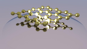 |
| The transparency of a device at the 2-D limit can be tuned using an electric bias, where different type of optical processes that simply define the way we see objects can be modify externally. This gives the control on properties that until very recently were not thought to be manipulated arbitrarily. CREDIT: Queen's University Belfast |
Abstract:
Researchers at Queen's University Belfast and ETH Zurich, Switzerland, have created a new theoretical framework which could help physicists and device engineers design better optoelectronics, leading to less heat generation and power consumption in electronic devices which source, detect, and control light.
New theory could lead to new generation of energy friendly optoelectronics: Researchers at Queen's University Belfast and ETH Zurich, Switzerland, have created a new theoretical framework which could help physicists and device engineers design better optoelectronics
Belfastm, Ireland | Posted on August 23rd, 2016Speaking about the research, which enables scientists and engineers to quantify how transparent a 2D material is to an electrostatic field, Dr Elton Santos from the Atomistic Simulation Research Centre at Queen's, said: "In our paper we have developed a theoretical framework that predicts and quantifies the degree of 'transparency' up to the limit of one-atom-thick, 2D materials, to an electrostatic field.
"Imagine we can change the transparency of a material just using an electric bias, e.g. get darker or brighter at will. What kind of implications would this have, for instance, in mobile phone technologies? This was the first question we asked ourselves. We realised that this would allow the microscopic control over the distribution of charged carriers in a bulk semiconductor (e.g. traditional Si microchips) in a nonlinear manner. This will help physicists and device engineers to design better quantum capacitors, an array of subatomic power storage components capable to keep high energy densities, for instance, in batteries, and vertical transistors, leading to next-generation optoelectronics with lower power consumption and dissipation of heat (cold devices), and better performance. In other words, smarter smart phones."
Explaining how the theory could have important implications for future work in the area, Dr Santos added: "Our current model simply considers an interface formed between a layer of 2D material and a bulk semiconductor. In principle, our approach can be readily extended to a stack of multiple 2D materials, or namely, van der Waals heterostructures recently fabricated. This will allow us to design and predict the behaviour of these cutting-edge devices in prior to actual fabrication, which will significantly facilitate developments for a variety of applications. We will have an in silico search for the right combination of different 2D crystals while reducing the need for expensive lab work and test trials."
The present multiscale approach considers the penetration of the field effect through a monolayer 2D material in a metal-oxide-2D material semiconductor (MOGS) quantum capacitor (QC). By using graphene as the model system, the team at Queen's and Zurich ETH developed a macroscopic model to describe the charge distribution in graphene and the semiconductor. These results are corroborated by atomistic ab initio calculations at the level of density functional theory, including van der Waals interactions, which are important due to the nanoscale of the problem (e.g. 10-9 m), and Poisson-Boltzmann equation methods, importantly at micro-scale (e.g. 10-6 m).
The team next defined and formulated an index or parameter that quantified the transparency of a monolayer 2D material to an electric displacement field and showed that the transparency is determined by the combined effect of 2D material quantum capacitance and the semiconductor capacitance (classical one studied in high-school). By calculating the quantum capacitance for a variety of 2D materials using accurate hybrid functionals, they predicted the ranking for a variety of 2D compounds according to their transparency to an electric displacement field as follows: graphene > silicene > germanene > WS2 > WTe2 > WSe2 > MoS2 > MoSe2 > MoTe2, when the majority carrier is electron.
Funding acknowledgements: E.J.G.S. acknowledges the use of computational resources from the UK national high performance computing service, ARCHER, for which access was obtained via the UKCP consortium and funded by EPSRC grant ref EP/K013564/1; and the Extreme Science and Engineering Discovery Environment (XSEDE), supported by NSF grants number TG-DMR120049 and TG-DMR150017. The Queen's Fellow Award through the startup grant number M8407MPH is also acknowledged and the PhD studentship from the Energy PRP funded by NI-DEL and Queen's University Belfast.
####
For more information, please click here
Contacts:
Anne-Marie Clarke
44-028-909-75310
Copyright © Queen's University Belfast
If you have a comment, please Contact us.Issuers of news releases, not 7th Wave, Inc. or Nanotechnology Now, are solely responsible for the accuracy of the content.
Bookmark:


| Related Links |
![]() Further information on the Atomistic Simulation Research Centre at Queen's is available online at:
Further information on the Atomistic Simulation Research Centre at Queen's is available online at:
| Related News Press |
News and information
![]() Quantum computer improves AI predictions April 17th, 2026
Quantum computer improves AI predictions April 17th, 2026
![]() Flexible sensor gains sensitivity under pressure April 17th, 2026
Flexible sensor gains sensitivity under pressure April 17th, 2026
![]() A reusable chip for particulate matter sensing April 17th, 2026
A reusable chip for particulate matter sensing April 17th, 2026
![]() Detecting vibrational quantum beating in the predissociation dynamics of SF6 using time-resolved photoelectron spectroscopy April 17th, 2026
Detecting vibrational quantum beating in the predissociation dynamics of SF6 using time-resolved photoelectron spectroscopy April 17th, 2026
Physics
![]() UC Irvine physicists discover method to reverse �quantum scrambling� : The work addresses the problem of information loss in quantum computing system April 17th, 2026
UC Irvine physicists discover method to reverse �quantum scrambling� : The work addresses the problem of information loss in quantum computing system April 17th, 2026
![]() Quantum computers simulate fundamental physics: shedding light on the building blocks of nature June 6th, 2025
Quantum computers simulate fundamental physics: shedding light on the building blocks of nature June 6th, 2025
Govt.-Legislation/Regulation/Funding/Policy
![]() Quantum computer improves AI predictions April 17th, 2026
Quantum computer improves AI predictions April 17th, 2026
![]() Metasurfaces smooth light to boost magnetic sensing precision January 30th, 2026
Metasurfaces smooth light to boost magnetic sensing precision January 30th, 2026
![]() New imaging approach transforms study of bacterial biofilms August 8th, 2025
New imaging approach transforms study of bacterial biofilms August 8th, 2025
Possible Futures
![]() A fundamentally new therapeutic approach to cystic fibrosis: Nanobody repairs cellular defect April 17th, 2026
A fundamentally new therapeutic approach to cystic fibrosis: Nanobody repairs cellular defect April 17th, 2026
![]() UC Irvine physicists discover method to reverse �quantum scrambling� : The work addresses the problem of information loss in quantum computing system April 17th, 2026
UC Irvine physicists discover method to reverse �quantum scrambling� : The work addresses the problem of information loss in quantum computing system April 17th, 2026
Chip Technology
![]() A reusable chip for particulate matter sensing April 17th, 2026
A reusable chip for particulate matter sensing April 17th, 2026
![]() Metasurfaces smooth light to boost magnetic sensing precision January 30th, 2026
Metasurfaces smooth light to boost magnetic sensing precision January 30th, 2026
Optical computing/Photonic computing
![]() ICFO researchers overcome long-standing bottleneck in single photon detection with twisted 2D materials August 8th, 2025
ICFO researchers overcome long-standing bottleneck in single photon detection with twisted 2D materials August 8th, 2025
![]() Programmable electron-induced color router array May 14th, 2025
Programmable electron-induced color router array May 14th, 2025
Discoveries
![]() Quantum computer improves AI predictions April 17th, 2026
Quantum computer improves AI predictions April 17th, 2026
![]() Flexible sensor gains sensitivity under pressure April 17th, 2026
Flexible sensor gains sensitivity under pressure April 17th, 2026
![]() A reusable chip for particulate matter sensing April 17th, 2026
A reusable chip for particulate matter sensing April 17th, 2026
![]() Detecting vibrational quantum beating in the predissociation dynamics of SF6 using time-resolved photoelectron spectroscopy April 17th, 2026
Detecting vibrational quantum beating in the predissociation dynamics of SF6 using time-resolved photoelectron spectroscopy April 17th, 2026
Announcements
![]() A fundamentally new therapeutic approach to cystic fibrosis: Nanobody repairs cellular defect April 17th, 2026
A fundamentally new therapeutic approach to cystic fibrosis: Nanobody repairs cellular defect April 17th, 2026
![]() UC Irvine physicists discover method to reverse �quantum scrambling� : The work addresses the problem of information loss in quantum computing system April 17th, 2026
UC Irvine physicists discover method to reverse �quantum scrambling� : The work addresses the problem of information loss in quantum computing system April 17th, 2026
Interviews/Book Reviews/Essays/Reports/Podcasts/Journals/White papers/Posters
![]() A fundamentally new therapeutic approach to cystic fibrosis: Nanobody repairs cellular defect April 17th, 2026
A fundamentally new therapeutic approach to cystic fibrosis: Nanobody repairs cellular defect April 17th, 2026
![]() UC Irvine physicists discover method to reverse �quantum scrambling� : The work addresses the problem of information loss in quantum computing system April 17th, 2026
UC Irvine physicists discover method to reverse �quantum scrambling� : The work addresses the problem of information loss in quantum computing system April 17th, 2026
Photonics/Optics/Lasers
![]() Metasurfaces smooth light to boost magnetic sensing precision January 30th, 2026
Metasurfaces smooth light to boost magnetic sensing precision January 30th, 2026
![]() From sensors to smart systems: the rise of AI-driven photonic noses January 30th, 2026
From sensors to smart systems: the rise of AI-driven photonic noses January 30th, 2026
Research partnerships
![]() Lab to industry: InSe wafer-scale breakthrough for future electronics August 8th, 2025
Lab to industry: InSe wafer-scale breakthrough for future electronics August 8th, 2025
![]() HKU physicists uncover hidden order in the quantum world through deconfined quantum critical points April 25th, 2025
HKU physicists uncover hidden order in the quantum world through deconfined quantum critical points April 25th, 2025
|
|
||
|
|
||
| The latest news from around the world, FREE | ||
|
|
||
|
|
||
| Premium Products | ||
|
|
||
|
Only the news you want to read!
Learn More |
||
|
|
||
|
Full-service, expert consulting
Learn More |
||
|
|
||