Home > Press > Unlocking nanofibers’ potential: Prototype boosts production of versatile fibers fourfold, while cutting energy consumption by 92 percent
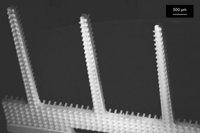 |
| A scanning electron micrograph of the new microfiber emitters, showing the arrays of rectangular columns etched into their sides.
Courtesy of the researchers |
Abstract:
Nanofibers — polymer filaments only a couple of hundred nanometers in diameter — have a huge range of potential applications, from solar cells to water filtration to fuel cells. But so far, their high cost of manufacture has relegated them to just a few niche industries.
Unlocking nanofibers’ potential: Prototype boosts production of versatile fibers fourfold, while cutting energy consumption by 92 percent
Cambridge, MA | Posted on June 5th, 2015In the latest issue of the journal Nanotechnology, MIT researchers describe a new technique for producing nanofibers that increases the rate of production fourfold while reducing energy consumption by more than 90 percent, holding out the prospect of cheap, efficient nanofiber production.
“We have demonstrated a systematic way to produce nanofibers through electrospinning that surpasses the state of the art,” says Luis Fernando Velásquez-García, a principal research scientist in MIT’s Microsystems Technology Laboratories, who led the new work. “But the way that it’s done opens a very interesting possibility. Our group and many other groups are working to push 3-D printing further, to make it possible to print components that transduce, that actuate, that exchange energy between different domains, like solar to electrical or mechanical. We have something that naturally fits into that picture. We have an array of emitters that can be thought of as a dot-matrix printer, where you would be able to individually control each emitter to print deposits of nanofibers.”
Tangled tale
Nanofibers are useful for any application that benefits from a high ratio of surface area to volume — solar cells, for instance, which try to maximize exposure to sunlight, or fuel cell electrodes, which catalyze reactions at their surfaces. Nanofibers can also yield materials that are permeable only at very small scales, like water filters, or that are remarkably tough for their weight, like body armor.
The standard technique for manufacturing nanofibers is called electrospinning, and it comes in two varieties. In the first, a polymer solution is pumped through a small nozzle, and then a strong electric field stretches it out. The process is slow, however, and the number of nozzles per unit area is limited by the size of the pump hydraulics.
The other approach is to apply a voltage between a rotating drum covered by metal cones and a collector electrode. The cones are dipped in a polymer solution, and the electric field causes the solution to travel to the top of the cones, where it’s emitted toward the electrode as a fiber. That approach is erratic, however, and produces fibers of uneven lengths; it also requires voltages as high as 100,000 volts.
Thinking small
Velásquez-García and his co-authors — Philip Ponce de Leon, a former master’s student in mechanical engineering; Frances Hill, a former postdoc in Velásquez-García’s group who’s now at KLA-Tencor; and Eric Heubel, a current postdoc — adapt the second approach, but on a much smaller scale, using techniques common in the manufacture of microelectromechanical systems to produce dense arrays of tiny emitters. The emitters’ small size reduces the voltage necessary to drive them and allows more of them to be packed together, increasing production rate.
At the same time, a nubbly texture etched into the emitters’ sides regulates the rate at which fluid flows toward their tips, yielding uniform fibers even at high manufacturing rates. “We did all kinds of experiments, and all of them show that the emission is uniform,” Velásquez-García says.
To build their emitters, Velásquez-García and his colleagues use a technique called deep reactive-ion etching. On either face of a silicon wafer, they etch dense arrays of tiny rectangular columns — tens of micrometers across — which will regulate the flow of fluid up the sides of the emitters. Then they cut sawtooth patterns out of the wafer. The sawteeth are mounted vertically, and their bases are immersed in a solution of deionized water, ethanol, and a dissolved polymer.
When an electrode is mounted opposite the sawteeth and a voltage applied between them, the water-ethanol mixture streams upward, dragging chains of polymer with it. The water and ethanol quickly dissolve, leaving a tangle of polymer filaments opposite each emitter, on the electrode.
The researchers were able to pack 225 emitters, several millimeters long, on a square chip about 35 millimeters on a side. At the relatively low voltage of 8,000 volts, that device yielded four times as much fiber per unit area as the best commercial electrospinning devices.
###
Written by Larry Hardesty, MIT News Office
####
For more information, please click here
Contacts:
Abby Abazorius
MIT News Office
617.253.2709
Copyright © Massachusetts Institute of Technology
If you have a comment, please Contact us.Issuers of news releases, not 7th Wave, Inc. or Nanotechnology Now, are solely responsible for the accuracy of the content.
Bookmark:


| Related Links |
| Related News Press |
News and information
![]() Quantum computer improves AI predictions April 17th, 2026
Quantum computer improves AI predictions April 17th, 2026
![]() Flexible sensor gains sensitivity under pressure April 17th, 2026
Flexible sensor gains sensitivity under pressure April 17th, 2026
![]() A reusable chip for particulate matter sensing April 17th, 2026
A reusable chip for particulate matter sensing April 17th, 2026
![]() Detecting vibrational quantum beating in the predissociation dynamics of SF6 using time-resolved photoelectron spectroscopy April 17th, 2026
Detecting vibrational quantum beating in the predissociation dynamics of SF6 using time-resolved photoelectron spectroscopy April 17th, 2026
Discoveries
![]() Quantum computer improves AI predictions April 17th, 2026
Quantum computer improves AI predictions April 17th, 2026
![]() Flexible sensor gains sensitivity under pressure April 17th, 2026
Flexible sensor gains sensitivity under pressure April 17th, 2026
![]() A reusable chip for particulate matter sensing April 17th, 2026
A reusable chip for particulate matter sensing April 17th, 2026
![]() Detecting vibrational quantum beating in the predissociation dynamics of SF6 using time-resolved photoelectron spectroscopy April 17th, 2026
Detecting vibrational quantum beating in the predissociation dynamics of SF6 using time-resolved photoelectron spectroscopy April 17th, 2026
Materials/Metamaterials/Magnetoresistance
![]() First real-time observation of two-dimensional melting process: Researchers at Mainz University unveil new insights into magnetic vortex structures August 8th, 2025
First real-time observation of two-dimensional melting process: Researchers at Mainz University unveil new insights into magnetic vortex structures August 8th, 2025
![]() Researchers unveil a groundbreaking clay-based solution to capture carbon dioxide and combat climate change June 6th, 2025
Researchers unveil a groundbreaking clay-based solution to capture carbon dioxide and combat climate change June 6th, 2025
![]() A 1960s idea inspires NBI researchers to study hitherto inaccessible quantum states June 6th, 2025
A 1960s idea inspires NBI researchers to study hitherto inaccessible quantum states June 6th, 2025
![]() Institute for Nanoscience hosts annual proposal planning meeting May 16th, 2025
Institute for Nanoscience hosts annual proposal planning meeting May 16th, 2025
Announcements
![]() A fundamentally new therapeutic approach to cystic fibrosis: Nanobody repairs cellular defect April 17th, 2026
A fundamentally new therapeutic approach to cystic fibrosis: Nanobody repairs cellular defect April 17th, 2026
![]() UC Irvine physicists discover method to reverse ‘quantum scrambling’ : The work addresses the problem of information loss in quantum computing system April 17th, 2026
UC Irvine physicists discover method to reverse ‘quantum scrambling’ : The work addresses the problem of information loss in quantum computing system April 17th, 2026
Interviews/Book Reviews/Essays/Reports/Podcasts/Journals/White papers/Posters
![]() A fundamentally new therapeutic approach to cystic fibrosis: Nanobody repairs cellular defect April 17th, 2026
A fundamentally new therapeutic approach to cystic fibrosis: Nanobody repairs cellular defect April 17th, 2026
![]() UC Irvine physicists discover method to reverse ‘quantum scrambling’ : The work addresses the problem of information loss in quantum computing system April 17th, 2026
UC Irvine physicists discover method to reverse ‘quantum scrambling’ : The work addresses the problem of information loss in quantum computing system April 17th, 2026
Energy
![]() Sensors innovations for smart lithium-based batteries: advancements, opportunities, and potential challenges August 8th, 2025
Sensors innovations for smart lithium-based batteries: advancements, opportunities, and potential challenges August 8th, 2025
![]() Simple algorithm paired with standard imaging tool could predict failure in lithium metal batteries August 8th, 2025
Simple algorithm paired with standard imaging tool could predict failure in lithium metal batteries August 8th, 2025
Water
![]() Taking salt out of the water equation October 7th, 2022
Taking salt out of the water equation October 7th, 2022
Industrial
![]() Tiny nanosheets, big leap: A new sensor detects ethanol at ultra-low levels January 30th, 2026
Tiny nanosheets, big leap: A new sensor detects ethanol at ultra-low levels January 30th, 2026
![]() Quantum interference in molecule-surface collisions February 28th, 2025
Quantum interference in molecule-surface collisions February 28th, 2025
![]() Boron nitride nanotube fibers get real: Rice lab creates first heat-tolerant, stable fibers from wet-spinning process June 24th, 2022
Boron nitride nanotube fibers get real: Rice lab creates first heat-tolerant, stable fibers from wet-spinning process June 24th, 2022
Fuel Cells
![]() Deciphering local microstrain-induced optimization of asymmetric Fe single atomic sites for efficient oxygen reduction August 8th, 2025
Deciphering local microstrain-induced optimization of asymmetric Fe single atomic sites for efficient oxygen reduction August 8th, 2025
![]() Current and Future Developments in Nanomaterials and Carbon Nanotubes: Applications of Nanomaterials in Energy Storage and Electronics October 28th, 2022
Current and Future Developments in Nanomaterials and Carbon Nanotubes: Applications of Nanomaterials in Energy Storage and Electronics October 28th, 2022
Solar/Photovoltaic
![]() Spinel-type sulfide semiconductors to operate the next-generation LEDs and solar cells For solar-cell absorbers and green-LED source October 3rd, 2025
Spinel-type sulfide semiconductors to operate the next-generation LEDs and solar cells For solar-cell absorbers and green-LED source October 3rd, 2025
![]() KAIST researchers introduce new and improved, next-generation perovskite solar cell November 8th, 2024
KAIST researchers introduce new and improved, next-generation perovskite solar cell November 8th, 2024
![]() Groundbreaking precision in single-molecule optoelectronics August 16th, 2024
Groundbreaking precision in single-molecule optoelectronics August 16th, 2024
![]() Development of zinc oxide nanopagoda array photoelectrode: photoelectrochemical water-splitting hydrogen production January 12th, 2024
Development of zinc oxide nanopagoda array photoelectrode: photoelectrochemical water-splitting hydrogen production January 12th, 2024
|
|
||
|
|
||
| The latest news from around the world, FREE | ||
|
|
||
|
|
||
| Premium Products | ||
|
|
||
|
Only the news you want to read!
Learn More |
||
|
|
||
|
Full-service, expert consulting
Learn More |
||
|
|
||