Home > Press > New pathway to valleytronics
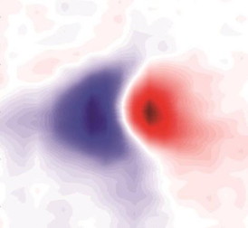 |
| A study has shown that the optical Stark effect, which describes the energy shift in a two-level system induced by a non-resonant laser field, can be used to control valley excitons in MX2 semiconductors. CREDIT: Image courtesy of Feng Wang, Berkeley Lab |
Abstract:
A potential avenue to quantum computing currently generating quite the buzz in the high-tech industry is "valleytronics," in which information is coded based on the wavelike motion of electrons moving through certain two-dimensional (2D) semiconductors. Now, a promising new pathway to valleytronic technology has been uncovered by researchers with the Lawrence Berkeley National Laboratory (Berkeley Lab).
New pathway to valleytronics
Berkeley, CA | Posted on January 27th, 2015Feng Wang, a condensed matter physicist with Berkeley Lab's Materials Sciences Division, led a study in which it was demonstrated that a well-established phenomenon known as the "optical Stark effect" can be used to selectively control photoexcited electrons/hole pairs - referred to as excitons -in different energy valleys. In valleytronics, electrons move through the lattice of a 2D semiconductor as a wave with two energy valleys, each valley being characterized by a distinct momentum and quantum valley number. This quantum valley number can be used to encode information when the electrons are in a minimum energy valley. The technique is analogous to spintronics, in which information is encoded in a quantum spin number.
"This is the first demonstration of the important role the optical Stark effect can play in valleytronics," Feng says. "Our technique, which is based on the use of circularly polarized femtosecond light pulses to selectively control the valley degree of freedom, opens up the possibility of ultrafast manipulation of valley excitons for quantum information applications."
Wang, who also holds an appointment with the University of California (UC) Berkeley Physics Department, has been working with the 2D semiconductors known as MX2 materials, monolayers consisting of a single layer of transition metal atoms, such as molybdenum (Mo) or tungsten (W), sandwiched between two layers of chalcogen atoms, such as sulfur (S). This family of atomically thin 2D semiconductors features the same hexagonal "honeycombed" lattice as graphene. Unlike graphene, however, MX2 materials have natural energy band-gaps that facilitate their use in transistors and other electronic devices.
This past year, Wang and his group reported the first experimental observation of ultrafast charge transfer in photo-excited MX2 materials. The recorded charge transfer time of less than 50 femtoseconds established MX2 materials as competitors with graphene for future electronic devices. In this new study, Wang and his group generated ultrafast and ultrahigh pseudo-magnetic fields for controlling valley excitons in triangular monolayers of WSe2 using the optical Stark effect.
"The optical Stark effect describes the energy shift in a two-level system induced by a non-resonant laser field," Wang says.
"Using ultrafast pump-probe spectroscopy, we were able to observe a pure and valley-selective optical Stark effect in WSe2 monolayers from the non-resonant pump that resulted in an energy splitting of more than 10 milli-electron volts between the K and K? valley exciton transitions. As controlling valley excitons with a real magnetic field is difficult to achieve even with superconducting magnets, a light-induced pseudo-magnetic field is highly desirable."
Like spintronics, valleytronics offer a tremendous advantage in data processing speeds over the electrical charge used in classical electronics. Quantum spin, however, is strongly linked to magnetic fields, which can introduce stability issues. This is not an issue for quantum waves.
"The valley-dependent optical Stark effect offers a convenient and ultrafast way of enabling the coherent rotation of resonantly excited valley polarizations with high fidelity," Wang says. "Such coherent manipulation of valley polarization should open up fascinating opportunities for valleytronics."
This research was funded by the U.S. Department of Energy's Office of Science.
####
About DOE/Lawrence Berkeley National Laboratory
Lawrence Berkeley National Laboratory addresses the world's most urgent scientific challenges by advancing sustainable energy, protecting human health, creating new materials, and revealing the origin and fate of the universe. Founded in 1931, Berkeley Lab's scientific expertise has been recognized with 13 Nobel prizes. The University of California manages Berkeley Lab for the U.S. Department of Energy's Office of Science. For more, visit http://www.lbl.gov.
DOE's Office of Science is the single largest supporter of basic research in the physical sciences in the United States, and is working to address some of the most pressing challenges of our time. For more information, please visit the Office of Science website at science.energy.gov/.
For more information, please click here
Contacts:
Lynn Yarris
510-486-5375
Copyright © DOE/Lawrence Berkeley National Laboratory
If you have a comment, please Contact us.Issuers of news releases, not 7th Wave, Inc. or Nanotechnology Now, are solely responsible for the accuracy of the content.
Bookmark:


| Related Links |
| Related News Press |
News and information
![]() Quantum computer improves AI predictions April 17th, 2026
Quantum computer improves AI predictions April 17th, 2026
![]() Flexible sensor gains sensitivity under pressure April 17th, 2026
Flexible sensor gains sensitivity under pressure April 17th, 2026
![]() A reusable chip for particulate matter sensing April 17th, 2026
A reusable chip for particulate matter sensing April 17th, 2026
![]() Detecting vibrational quantum beating in the predissociation dynamics of SF6 using time-resolved photoelectron spectroscopy April 17th, 2026
Detecting vibrational quantum beating in the predissociation dynamics of SF6 using time-resolved photoelectron spectroscopy April 17th, 2026
Physics
![]() UC Irvine physicists discover method to reverse �quantum scrambling� : The work addresses the problem of information loss in quantum computing system April 17th, 2026
UC Irvine physicists discover method to reverse �quantum scrambling� : The work addresses the problem of information loss in quantum computing system April 17th, 2026
![]() Quantum computers simulate fundamental physics: shedding light on the building blocks of nature June 6th, 2025
Quantum computers simulate fundamental physics: shedding light on the building blocks of nature June 6th, 2025
![]() A 1960s idea inspires NBI researchers to study hitherto inaccessible quantum states June 6th, 2025
A 1960s idea inspires NBI researchers to study hitherto inaccessible quantum states June 6th, 2025
Laboratories
![]() Researchers develop molecular qubits that communicate at telecom frequencies October 3rd, 2025
Researchers develop molecular qubits that communicate at telecom frequencies October 3rd, 2025
Govt.-Legislation/Regulation/Funding/Policy
![]() Quantum computer improves AI predictions April 17th, 2026
Quantum computer improves AI predictions April 17th, 2026
![]() Metasurfaces smooth light to boost magnetic sensing precision January 30th, 2026
Metasurfaces smooth light to boost magnetic sensing precision January 30th, 2026
![]() New imaging approach transforms study of bacterial biofilms August 8th, 2025
New imaging approach transforms study of bacterial biofilms August 8th, 2025
Chip Technology
![]() A reusable chip for particulate matter sensing April 17th, 2026
A reusable chip for particulate matter sensing April 17th, 2026
![]() Metasurfaces smooth light to boost magnetic sensing precision January 30th, 2026
Metasurfaces smooth light to boost magnetic sensing precision January 30th, 2026
Quantum Computing
![]() Quantum computer improves AI predictions April 17th, 2026
Quantum computer improves AI predictions April 17th, 2026
![]() UC Irvine physicists discover method to reverse �quantum scrambling� : The work addresses the problem of information loss in quantum computing system April 17th, 2026
UC Irvine physicists discover method to reverse �quantum scrambling� : The work addresses the problem of information loss in quantum computing system April 17th, 2026
![]() Researchers develop molecular qubits that communicate at telecom frequencies October 3rd, 2025
Researchers develop molecular qubits that communicate at telecom frequencies October 3rd, 2025
Discoveries
![]() Quantum computer improves AI predictions April 17th, 2026
Quantum computer improves AI predictions April 17th, 2026
![]() Flexible sensor gains sensitivity under pressure April 17th, 2026
Flexible sensor gains sensitivity under pressure April 17th, 2026
![]() A reusable chip for particulate matter sensing April 17th, 2026
A reusable chip for particulate matter sensing April 17th, 2026
![]() Detecting vibrational quantum beating in the predissociation dynamics of SF6 using time-resolved photoelectron spectroscopy April 17th, 2026
Detecting vibrational quantum beating in the predissociation dynamics of SF6 using time-resolved photoelectron spectroscopy April 17th, 2026
Announcements
![]() A fundamentally new therapeutic approach to cystic fibrosis: Nanobody repairs cellular defect April 17th, 2026
A fundamentally new therapeutic approach to cystic fibrosis: Nanobody repairs cellular defect April 17th, 2026
![]() UC Irvine physicists discover method to reverse �quantum scrambling� : The work addresses the problem of information loss in quantum computing system April 17th, 2026
UC Irvine physicists discover method to reverse �quantum scrambling� : The work addresses the problem of information loss in quantum computing system April 17th, 2026
Interviews/Book Reviews/Essays/Reports/Podcasts/Journals/White papers/Posters
![]() A fundamentally new therapeutic approach to cystic fibrosis: Nanobody repairs cellular defect April 17th, 2026
A fundamentally new therapeutic approach to cystic fibrosis: Nanobody repairs cellular defect April 17th, 2026
![]() UC Irvine physicists discover method to reverse �quantum scrambling� : The work addresses the problem of information loss in quantum computing system April 17th, 2026
UC Irvine physicists discover method to reverse �quantum scrambling� : The work addresses the problem of information loss in quantum computing system April 17th, 2026
Photonics/Optics/Lasers
![]() Metasurfaces smooth light to boost magnetic sensing precision January 30th, 2026
Metasurfaces smooth light to boost magnetic sensing precision January 30th, 2026
![]() From sensors to smart systems: the rise of AI-driven photonic noses January 30th, 2026
From sensors to smart systems: the rise of AI-driven photonic noses January 30th, 2026
Quantum nanoscience
![]() Beyond silicon: Electronics at the scale of a single molecule January 30th, 2026
Beyond silicon: Electronics at the scale of a single molecule January 30th, 2026
![]() MXene nanomaterials enter a new dimension Multilayer nanomaterial: MXene flakes created at Drexel University show new promise as 1D scrolls January 30th, 2026
MXene nanomaterials enter a new dimension Multilayer nanomaterial: MXene flakes created at Drexel University show new promise as 1D scrolls January 30th, 2026
![]() ICFO researchers overcome long-standing bottleneck in single photon detection with twisted 2D materials August 8th, 2025
ICFO researchers overcome long-standing bottleneck in single photon detection with twisted 2D materials August 8th, 2025
|
|
||
|
|
||
| The latest news from around the world, FREE | ||
|
|
||
|
|
||
| Premium Products | ||
|
|
||
|
Only the news you want to read!
Learn More |
||
|
|
||
|
Full-service, expert consulting
Learn More |
||
|
|
||