Home > Press > 'Giant' charge density disturbances discovered in nanomaterials: Juelich researchers amplify Friedel oscillations in thin metallic films
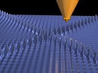 |
| Electron density oscillations on the surface of a metallic film were made visible with the help of low temperature scanning tunneling microscopy.
Credit: Forschungszentrum Jülich |
Abstract:
In metals such as copper or aluminium, so-called conduction electrons are able to move around freely, in the same way as particles in a gas or a liquid. If, however, impurities are implanted into the metal's crystal lattice, the electrons cluster together in a uniform pattern around the point of interference, resembling the ripples that occur when a stone is thrown into a pool of water. Scientists in Jülich have, with the help of computer simulations, now discovered a combination of materials that strengthens these Friedel oscillations and bundles them, as if with a lens, in different directions. With a range of 50 nanometers, these "giant anisotropic charge density oscillations" are many times greater than normal and open up new possibilities in the field of nanoelectronics to exchange or filter magnetic information. (Nature Communications, DOI: 10.1038/ncomms6558)
'Giant' charge density disturbances discovered in nanomaterials: Juelich researchers amplify Friedel oscillations in thin metallic films
Juelich, Germany | Posted on November 26th, 2014The study just published in "Nature Communications" was preceded by an extraordinary discovery: scientists at the Peter Grünberg Institute in Jülich noticed oddly-shaped electron waves in images obtained using scanning tunnelling microscopy. The pictures showed the surface of a thin film of iron with oxygen impurities. "The wave pattern did not consist of closed rings as one would normally expect, but rather spread out crosswise from the point of interference in four different directions", reported Dr. Samir Lounis.
The reason for the unusual distribution of the electron density fluctuations is the virtually square-shaped Fermi surfaces of the material. The electrons with the most energy in an atomic compound are the ones which move about on the Fermi surfaces. The shape of the Fermi surfaces and the mobility of the electrons determine the physical properties of the metals. Fermi surfaces are often circular or square-shaped with rounded edges.
"The virtually flat Fermi surfaces of our samples act as an amplifier for Friedel oscillations, which spread out perpendicular to the surfaces", explains Lounis. The researchers have found out that this effect can be substantially intensified by varying the thickness of the metal. Depending on the number of atomic layers present, piles of Fermi surfaces are formed; the more of them there are, the greater the oscillations. The researchers called this effect the "Giant Anisotropic Charge Density Oscillations".
In principle, the oscillations could be used to exchange information between individual magnetic impurities and further enhance the level of integration of nanoelectronic components. As the oscillations are mainly produced by spins of a single orientation, they could also form the basis for so-called spin filter elements, which are important components in spintronic applications.
####
For more information, please click here
Contacts:
Angela Wenzik
49-246-161-6048
Contact:
Dr. Samir Lounis
Quantum Theory of Materials
(PGI-1/IAS-1)
Forschungszentrum Jülich
Phone: +49 24 61 61-6106
Copyright © Forschungszentrum Juelich
If you have a comment, please Contact us.Issuers of news releases, not 7th Wave, Inc. or Nanotechnology Now, are solely responsible for the accuracy of the content.
Bookmark:


| Related Links |
![]() Press release „Nano-Sonar Uses Electrons to Measure under the Surface" 27.2.2009:
Press release „Nano-Sonar Uses Electrons to Measure under the Surface" 27.2.2009:
![]() Institute: "Quantum Theory of Materials" (PGI-1/IAS-1):
Institute: "Quantum Theory of Materials" (PGI-1/IAS-1):
| Related News Press |
News and information
![]() Quantum computer improves AI predictions April 17th, 2026
Quantum computer improves AI predictions April 17th, 2026
![]() Flexible sensor gains sensitivity under pressure April 17th, 2026
Flexible sensor gains sensitivity under pressure April 17th, 2026
![]() A reusable chip for particulate matter sensing April 17th, 2026
A reusable chip for particulate matter sensing April 17th, 2026
![]() Detecting vibrational quantum beating in the predissociation dynamics of SF6 using time-resolved photoelectron spectroscopy April 17th, 2026
Detecting vibrational quantum beating in the predissociation dynamics of SF6 using time-resolved photoelectron spectroscopy April 17th, 2026
Thin films
![]() Tiny nanosheets, big leap: A new sensor detects ethanol at ultra-low levels January 30th, 2026
Tiny nanosheets, big leap: A new sensor detects ethanol at ultra-low levels January 30th, 2026
![]() Utilizing palladium for addressing contact issues of buried oxide thin film transistors April 5th, 2024
Utilizing palladium for addressing contact issues of buried oxide thin film transistors April 5th, 2024
![]() Understanding the mechanism of non-uniform formation of diamond film on tools: Paving the way to a dry process with less environmental impact March 24th, 2023
Understanding the mechanism of non-uniform formation of diamond film on tools: Paving the way to a dry process with less environmental impact March 24th, 2023
![]() New study introduces the best graphite films: The work by Distinguished Professor Feng Ding at UNIST has been published in the October 2022 issue of Nature Nanotechnology November 4th, 2022
New study introduces the best graphite films: The work by Distinguished Professor Feng Ding at UNIST has been published in the October 2022 issue of Nature Nanotechnology November 4th, 2022
Spintronics
![]() Quantum materials: Electron spin measured for the first time June 9th, 2023
Quantum materials: Electron spin measured for the first time June 9th, 2023
Chip Technology
![]() A reusable chip for particulate matter sensing April 17th, 2026
A reusable chip for particulate matter sensing April 17th, 2026
![]() Metasurfaces smooth light to boost magnetic sensing precision January 30th, 2026
Metasurfaces smooth light to boost magnetic sensing precision January 30th, 2026
Memory Technology
![]() Researchers tackle the memory bottleneck stalling quantum computing October 3rd, 2025
Researchers tackle the memory bottleneck stalling quantum computing October 3rd, 2025
![]() First real-time observation of two-dimensional melting process: Researchers at Mainz University unveil new insights into magnetic vortex structures August 8th, 2025
First real-time observation of two-dimensional melting process: Researchers at Mainz University unveil new insights into magnetic vortex structures August 8th, 2025
![]() Utilizing palladium for addressing contact issues of buried oxide thin film transistors April 5th, 2024
Utilizing palladium for addressing contact issues of buried oxide thin film transistors April 5th, 2024
Nanoelectronics
![]() Lab to industry: InSe wafer-scale breakthrough for future electronics August 8th, 2025
Lab to industry: InSe wafer-scale breakthrough for future electronics August 8th, 2025
![]() Interdisciplinary: Rice team tackles the future of semiconductors Multiferroics could be the key to ultralow-energy computing October 6th, 2023
Interdisciplinary: Rice team tackles the future of semiconductors Multiferroics could be the key to ultralow-energy computing October 6th, 2023
![]() Key element for a scalable quantum computer: Physicists from Forschungszentrum Jülich and RWTH Aachen University demonstrate electron transport on a quantum chip September 23rd, 2022
Key element for a scalable quantum computer: Physicists from Forschungszentrum Jülich and RWTH Aachen University demonstrate electron transport on a quantum chip September 23rd, 2022
![]() Reduced power consumption in semiconductor devices September 23rd, 2022
Reduced power consumption in semiconductor devices September 23rd, 2022
Discoveries
![]() Quantum computer improves AI predictions April 17th, 2026
Quantum computer improves AI predictions April 17th, 2026
![]() Flexible sensor gains sensitivity under pressure April 17th, 2026
Flexible sensor gains sensitivity under pressure April 17th, 2026
![]() A reusable chip for particulate matter sensing April 17th, 2026
A reusable chip for particulate matter sensing April 17th, 2026
![]() Detecting vibrational quantum beating in the predissociation dynamics of SF6 using time-resolved photoelectron spectroscopy April 17th, 2026
Detecting vibrational quantum beating in the predissociation dynamics of SF6 using time-resolved photoelectron spectroscopy April 17th, 2026
Materials/Metamaterials/Magnetoresistance
![]() First real-time observation of two-dimensional melting process: Researchers at Mainz University unveil new insights into magnetic vortex structures August 8th, 2025
First real-time observation of two-dimensional melting process: Researchers at Mainz University unveil new insights into magnetic vortex structures August 8th, 2025
![]() Researchers unveil a groundbreaking clay-based solution to capture carbon dioxide and combat climate change June 6th, 2025
Researchers unveil a groundbreaking clay-based solution to capture carbon dioxide and combat climate change June 6th, 2025
![]() A 1960s idea inspires NBI researchers to study hitherto inaccessible quantum states June 6th, 2025
A 1960s idea inspires NBI researchers to study hitherto inaccessible quantum states June 6th, 2025
![]() Institute for Nanoscience hosts annual proposal planning meeting May 16th, 2025
Institute for Nanoscience hosts annual proposal planning meeting May 16th, 2025
Announcements
![]() A fundamentally new therapeutic approach to cystic fibrosis: Nanobody repairs cellular defect April 17th, 2026
A fundamentally new therapeutic approach to cystic fibrosis: Nanobody repairs cellular defect April 17th, 2026
![]() UC Irvine physicists discover method to reverse ‘quantum scrambling’ : The work addresses the problem of information loss in quantum computing system April 17th, 2026
UC Irvine physicists discover method to reverse ‘quantum scrambling’ : The work addresses the problem of information loss in quantum computing system April 17th, 2026
Interviews/Book Reviews/Essays/Reports/Podcasts/Journals/White papers/Posters
![]() A fundamentally new therapeutic approach to cystic fibrosis: Nanobody repairs cellular defect April 17th, 2026
A fundamentally new therapeutic approach to cystic fibrosis: Nanobody repairs cellular defect April 17th, 2026
![]() UC Irvine physicists discover method to reverse ‘quantum scrambling’ : The work addresses the problem of information loss in quantum computing system April 17th, 2026
UC Irvine physicists discover method to reverse ‘quantum scrambling’ : The work addresses the problem of information loss in quantum computing system April 17th, 2026
|
|
||
|
|
||
| The latest news from around the world, FREE | ||
|
|
||
|
|
||
| Premium Products | ||
|
|
||
|
Only the news you want to read!
Learn More |
||
|
|
||
|
Full-service, expert consulting
Learn More |
||
|
|
||