Home > Press > Unconventional photoconduction in an atomically thin semiconductor: New mechanism of photoconduction could lead to next-generation excitonic devices
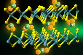 |
| Shown here is the crystal structure of molybdenum disulfide, MoS2, with molybdenum atoms shown in blue and sulfur atoms in yellow. When hit with a burst of laser light, freed electrons and holes combine to form combinations called trions, consisting of two electrons and one hole, and represented here by orange and green balls.
Illustration: Jose-Luis Olivares/MIT |
Abstract:
It's a well-known phenomenon in electronics: Shining light on a semiconductor, such as the silicon used in computer chips and solar cells, will make it more conductive. But now researchers have discovered that in a special semiconductor, light can have the opposite effect, making the material less conductive instead.
Unconventional photoconduction in an atomically thin semiconductor: New mechanism of photoconduction could lead to next-generation excitonic devices
Cambridge, MA | Posted on October 9th, 2014The phenomenon was discovered in an exotic two-dimensional semiconductor � a single layer of molybdenum disulfide (MoS2) just three atoms thick. The finding is reported in a paper in Physical Review Letters by MIT postdoc Joshua Lui; Nuh Gedik, the Lawrence C. and Sarah W. Biedenharn Career Development Associate Professor of Physics; and six others at MIT, Harvard University, and in Taiwan.
The researchers found that when illuminated by intense laser pulses, single-layer MoS2 is reduced to approximately one-third of its initial conductivity. The team used optical laser pulses to generate the effect and time-delayed terahertz pulses to detect the conductive response of the material.
"By measuring the transmission of the terahertz radiation through the material, we can extract its electrical conductivity," Gedik says. "This approach is more convenient than conventional methods that attach electrical contacts to the samples and measure the current."
When a semiconductor is illuminated by light, its conductivity tends to increase. This is because light absorption generates pairs of loose electrons and holes � places in a material with "missing" electrons � that facilitate the flow of electrical current through the material. This phenomenon has been the basis for designing and optimizing optoelectronic devices such as solar cells, digital cameras, and other light detectors.
The MIT team, however, observed the opposite behavior in a two-dimensional semiconductor. "Atomically thin layered crystals have been the subject of intense research in recent years," Lui says. "One remarkable property of these materials is the strong confinement of charge carriers in a two-dimensional plane. � As a consequence, the electrostatic interactions between the charge carriers are much stronger than those in three-dimensional solids."
The strong electrostatic interactions give rise to an interesting effect: When light generates an electron-hole pair in the material, instead of flying off freely as they would in a three-dimensional solid, they remain bound together. Such a bound state is called an exciton.
In fact, the interactions in single-layer MoS2 are so strong that excitons can capture extra free electrons in the material and form bound states with two electrons and one hole.
"These complex particles are called trions," Lui says. "They are analogous to negatively charged hydrogen ions, which consist of two electrons and one proton."
In single-layer MoS2, trions have the same net charge as an electron, but a mass roughly three times that of an electron. "Their much heavier mass dulls their response to the electric field, and lowers the material's conductivity," Lui says.
Instead of increasing the population of free charges, the illumination actually converts the original free electrons into heavier trions with the same charge density. This is the reason for the reduction of conductivity of single-layer MoS2 under illumination.
"This is a new mechanism of photoconduction in semiconductors," Gedik says, "which has not been observed before."
"Although negative photoconductivity has been reported in some semiconducting systems, it always arises from extrinsic factors, such as defects," Lui adds. "In this case, it is an intrinsic property of the crystal."
Trions are known to be unstable particles that usually appear at very low temperature and last for an extremely short period of time � so it has been very challenging to detect their influence on materials' conductivity. "In single-layer MoS2, the trionic effect is so strong that we can see it even at room temperature," Lui says. "Although the trions live for less than a billionth of a second, our ultrafast terahertz technique can detect them before they decay."
Gedik says that the work "might help us to realize room-temperature excitonic devices," which would otherwise require extremely low temperatures. In addition, because the effect can be switched on and off using light pulses, such devices could be easy to control without wired connections.
So far, the team has only studied the effect in MoS2, which belongs to a family of new two-dimensional semiconductors. "There are other types of two-dimensional materials with [similarly] strong trionic effect." Lui says. "They are likely to exhibit the same photoconduction phenomenon".
Xiaodong Xu, a professor of physics at the University of Washington who was not involved in this research, says it is "a piece of interesting and solid work." He adds, "This result is another evidence of strong Coulomb interaction in MoS2, consistent with previous studies of robust trions in monolayer transition metal dichalcogenides."
The research was supported by the U.S. Department of Energy and the National Science Foundation.
####
For more information, please click here
Contacts:
Andrew Carleen
Phone: 617-253-1682
Copyright © Massachusetts Institute of Technology
If you have a comment, please Contact us.Issuers of news releases, not 7th Wave, Inc. or Nanotechnology Now, are solely responsible for the accuracy of the content.
Bookmark:


| Related News Press |
News and information
![]() Quantum computer improves AI predictions April 17th, 2026
Quantum computer improves AI predictions April 17th, 2026
![]() Flexible sensor gains sensitivity under pressure April 17th, 2026
Flexible sensor gains sensitivity under pressure April 17th, 2026
![]() A reusable chip for particulate matter sensing April 17th, 2026
A reusable chip for particulate matter sensing April 17th, 2026
![]() Detecting vibrational quantum beating in the predissociation dynamics of SF6 using time-resolved photoelectron spectroscopy April 17th, 2026
Detecting vibrational quantum beating in the predissociation dynamics of SF6 using time-resolved photoelectron spectroscopy April 17th, 2026
Physics
![]() UC Irvine physicists discover method to reverse �quantum scrambling� : The work addresses the problem of information loss in quantum computing system April 17th, 2026
UC Irvine physicists discover method to reverse �quantum scrambling� : The work addresses the problem of information loss in quantum computing system April 17th, 2026
![]() Quantum computers simulate fundamental physics: shedding light on the building blocks of nature June 6th, 2025
Quantum computers simulate fundamental physics: shedding light on the building blocks of nature June 6th, 2025
![]() A 1960s idea inspires NBI researchers to study hitherto inaccessible quantum states June 6th, 2025
A 1960s idea inspires NBI researchers to study hitherto inaccessible quantum states June 6th, 2025
![]() Magnetism in new exotic material opens the way for robust quantum computers June 4th, 2025
Magnetism in new exotic material opens the way for robust quantum computers June 4th, 2025
Graphene/ Graphite
![]() Electrifying results shed light on graphene foam as a potential material for lab grown cartilage June 6th, 2025
Electrifying results shed light on graphene foam as a potential material for lab grown cartilage June 6th, 2025
Govt.-Legislation/Regulation/Funding/Policy
![]() Quantum computer improves AI predictions April 17th, 2026
Quantum computer improves AI predictions April 17th, 2026
![]() Metasurfaces smooth light to boost magnetic sensing precision January 30th, 2026
Metasurfaces smooth light to boost magnetic sensing precision January 30th, 2026
![]() New imaging approach transforms study of bacterial biofilms August 8th, 2025
New imaging approach transforms study of bacterial biofilms August 8th, 2025
Chip Technology
![]() A reusable chip for particulate matter sensing April 17th, 2026
A reusable chip for particulate matter sensing April 17th, 2026
![]() Metasurfaces smooth light to boost magnetic sensing precision January 30th, 2026
Metasurfaces smooth light to boost magnetic sensing precision January 30th, 2026
Discoveries
![]() Quantum computer improves AI predictions April 17th, 2026
Quantum computer improves AI predictions April 17th, 2026
![]() Flexible sensor gains sensitivity under pressure April 17th, 2026
Flexible sensor gains sensitivity under pressure April 17th, 2026
![]() A reusable chip for particulate matter sensing April 17th, 2026
A reusable chip for particulate matter sensing April 17th, 2026
![]() Detecting vibrational quantum beating in the predissociation dynamics of SF6 using time-resolved photoelectron spectroscopy April 17th, 2026
Detecting vibrational quantum beating in the predissociation dynamics of SF6 using time-resolved photoelectron spectroscopy April 17th, 2026
Announcements
![]() A fundamentally new therapeutic approach to cystic fibrosis: Nanobody repairs cellular defect April 17th, 2026
A fundamentally new therapeutic approach to cystic fibrosis: Nanobody repairs cellular defect April 17th, 2026
![]() UC Irvine physicists discover method to reverse �quantum scrambling� : The work addresses the problem of information loss in quantum computing system April 17th, 2026
UC Irvine physicists discover method to reverse �quantum scrambling� : The work addresses the problem of information loss in quantum computing system April 17th, 2026
|
|
||
|
|
||
| The latest news from around the world, FREE | ||
|
|
||
|
|
||
| Premium Products | ||
|
|
||
|
Only the news you want to read!
Learn More |
||
|
|
||
|
Full-service, expert consulting
Learn More |
||
|
|
||