Home > Press > Two-dimensional material shows promise for optoelectronics: Team creates LEDs, photovoltaic cells, and light detectors using novel 1-molecule-thick material
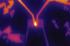 |
| In the team's experimental setup, electricity was supplied to a tiny piece of tungsten selenide (small rectangle at center) through two gold wires (from top left and right), causing it to emit light (bright area at center), demonstrating its potential as an LED material. IMAGE COURTESY OF BRITT BAUGHER AND HUGH CHURCHILL |
Abstract:
A team of MIT researchers has used a novel material that's just a few atoms thick to create devices that can harness or emit light. This proof-of-concept could lead to ultrathin, lightweight, and flexible photovoltaic cells, light emitting diodes (LEDs), and other optoelectronic devices, they say.
Two-dimensional material shows promise for optoelectronics: Team creates LEDs, photovoltaic cells, and light detectors using novel 1-molecule-thick material
Cambridge, MA | Posted on March 10th, 2014Their report is one of three papers by different groups describing similar results with this material, published in the March 9 issue of Nature Nanotechnology. The MIT research was carried out by Pablo Jarillo-Herrero, the Mitsui Career Development Associate Professor of Physics, graduate students Britton Baugher and Yafang Yang, and postdoc Hugh Churchill.
The material they used, called tungsten diselenide (WSe2), is part of a class of single-molecule-thick materials under investigation for possible use in new optoelectronic devices � ones that can manipulate the interactions of light and electricity. In these experiments, the MIT researchers were able to use the material to produce diodes, the basic building block of modern electronics.
Typically, diodes (which allow electrons to flow in only one direction) are made by "doping," which is a process of injecting other atoms into the crystal structure of a host material. By using different materials for this irreversible process, it is possible to make either of the two basic kinds of semiconducting materials, p-type or n-type.
But with the new material, either p-type or n-type functions can be obtained just by bringing the vanishingly thin film into very close proximity with an adjacent metal electrode, and tuning the voltage in this electrode from positive to negative. That means the material can easily and instantly be switched from one type to the other, which is rarely the case with conventional semiconductors.
In their experiments, the MIT team produced a device with a sheet of WSe2 material that was electrically doped half n-type and half p-type, creating a working diode that has properties "very close to the ideal," Jarillo-Herrero says.
By making diodes, it is possible to produce all three basic optoelectronic devices � photodetectors, photovoltaic cells, and LEDs; the MIT team has demonstrated all three, Jarillo-Herrero says. While these are proof-of-concept devices, and not designed for scaling up, the successful demonstration could point the way toward a wide range of potential uses, he says.
"It's known how to make very large-area materials" of this type, Churchill says. While further work will be required, he says, "there's no reason you wouldn't be able to do it on an industrial scale."
In principle, Jarillo-Herrero says, because this material can be engineered to produce different values of a key property called bandgap, it should be possible to make LEDs that produce any color � something that is difficult to do with conventional materials. And because the material is so thin, transparent, and lightweight, devices such as solar cells or displays could potentially be built into building or vehicle windows, or even incorporated into clothing, he says.
While selenium is not as abundant as silicon or other promising materials for electronics, the thinness of these sheets is a big advantage, Churchill points out: "It's thousands or tens of thousands of times thinner" than conventional diode materials, "so you'd use thousands of times less material" to make devices of a given size.
In addition to the diodes the team has produced, the team has also used the same methods to make p-type and n-type transistors and other electronic components, Jarillo-Herrero says. Such transistors could have a significant advantage in speed and power consumption because they are so thin, he says.
###
The research was supported by the U.S. Office of Naval Research, by a Packard fellowship, and by a Pappalardo fellowship, and made use of National Science Foundation-supported facilities.
Written by David L. Chandler, MIT News Office
####
For more information, please click here
Contacts:
Abby Abazorius
617-253-2709
Copyright © Massachusetts Institute of Technology
If you have a comment, please Contact us.Issuers of news releases, not 7th Wave, Inc. or Nanotechnology Now, are solely responsible for the accuracy of the content.
Bookmark:


| Related Links |
![]() Archive: Stacking 2-D materials produces surprising results:
Archive: Stacking 2-D materials produces surprising results:
| Related News Press |
News and information
![]() Quantum computer improves AI predictions April 17th, 2026
Quantum computer improves AI predictions April 17th, 2026
![]() Flexible sensor gains sensitivity under pressure April 17th, 2026
Flexible sensor gains sensitivity under pressure April 17th, 2026
![]() A reusable chip for particulate matter sensing April 17th, 2026
A reusable chip for particulate matter sensing April 17th, 2026
![]() Detecting vibrational quantum beating in the predissociation dynamics of SF6 using time-resolved photoelectron spectroscopy April 17th, 2026
Detecting vibrational quantum beating in the predissociation dynamics of SF6 using time-resolved photoelectron spectroscopy April 17th, 2026
Display technology/LEDs/SS Lighting/OLEDs
![]() Spinel-type sulfide semiconductors to operate the next-generation LEDs and solar cells For solar-cell absorbers and green-LED source October 3rd, 2025
Spinel-type sulfide semiconductors to operate the next-generation LEDs and solar cells For solar-cell absorbers and green-LED source October 3rd, 2025
![]() Efficient and stable hybrid perovskite-organic light-emitting diodes with external quantum efficiency exceeding 40 per cent July 5th, 2024
Efficient and stable hybrid perovskite-organic light-emitting diodes with external quantum efficiency exceeding 40 per cent July 5th, 2024
Govt.-Legislation/Regulation/Funding/Policy
![]() Quantum computer improves AI predictions April 17th, 2026
Quantum computer improves AI predictions April 17th, 2026
![]() Metasurfaces smooth light to boost magnetic sensing precision January 30th, 2026
Metasurfaces smooth light to boost magnetic sensing precision January 30th, 2026
![]() New imaging approach transforms study of bacterial biofilms August 8th, 2025
New imaging approach transforms study of bacterial biofilms August 8th, 2025
Chip Technology
![]() A reusable chip for particulate matter sensing April 17th, 2026
A reusable chip for particulate matter sensing April 17th, 2026
![]() Metasurfaces smooth light to boost magnetic sensing precision January 30th, 2026
Metasurfaces smooth light to boost magnetic sensing precision January 30th, 2026
Optical computing/Photonic computing
![]() ICFO researchers overcome long-standing bottleneck in single photon detection with twisted 2D materials August 8th, 2025
ICFO researchers overcome long-standing bottleneck in single photon detection with twisted 2D materials August 8th, 2025
![]() Programmable electron-induced color router array May 14th, 2025
Programmable electron-induced color router array May 14th, 2025
Nanoelectronics
![]() Lab to industry: InSe wafer-scale breakthrough for future electronics August 8th, 2025
Lab to industry: InSe wafer-scale breakthrough for future electronics August 8th, 2025
![]() Interdisciplinary: Rice team tackles the future of semiconductors Multiferroics could be the key to ultralow-energy computing October 6th, 2023
Interdisciplinary: Rice team tackles the future of semiconductors Multiferroics could be the key to ultralow-energy computing October 6th, 2023
![]() Key element for a scalable quantum computer: Physicists from Forschungszentrum J�lich and RWTH Aachen University demonstrate electron transport on a quantum chip September 23rd, 2022
Key element for a scalable quantum computer: Physicists from Forschungszentrum J�lich and RWTH Aachen University demonstrate electron transport on a quantum chip September 23rd, 2022
![]() Reduced power consumption in semiconductor devices September 23rd, 2022
Reduced power consumption in semiconductor devices September 23rd, 2022
Announcements
![]() A fundamentally new therapeutic approach to cystic fibrosis: Nanobody repairs cellular defect April 17th, 2026
A fundamentally new therapeutic approach to cystic fibrosis: Nanobody repairs cellular defect April 17th, 2026
![]() UC Irvine physicists discover method to reverse �quantum scrambling� : The work addresses the problem of information loss in quantum computing system April 17th, 2026
UC Irvine physicists discover method to reverse �quantum scrambling� : The work addresses the problem of information loss in quantum computing system April 17th, 2026
Interviews/Book Reviews/Essays/Reports/Podcasts/Journals/White papers/Posters
![]() A fundamentally new therapeutic approach to cystic fibrosis: Nanobody repairs cellular defect April 17th, 2026
A fundamentally new therapeutic approach to cystic fibrosis: Nanobody repairs cellular defect April 17th, 2026
![]() UC Irvine physicists discover method to reverse �quantum scrambling� : The work addresses the problem of information loss in quantum computing system April 17th, 2026
UC Irvine physicists discover method to reverse �quantum scrambling� : The work addresses the problem of information loss in quantum computing system April 17th, 2026
Energy
![]() Sensors innovations for smart lithium-based batteries: advancements, opportunities, and potential challenges August 8th, 2025
Sensors innovations for smart lithium-based batteries: advancements, opportunities, and potential challenges August 8th, 2025
![]() Simple algorithm paired with standard imaging tool could predict failure in lithium metal batteries August 8th, 2025
Simple algorithm paired with standard imaging tool could predict failure in lithium metal batteries August 8th, 2025
Photonics/Optics/Lasers
![]() Metasurfaces smooth light to boost magnetic sensing precision January 30th, 2026
Metasurfaces smooth light to boost magnetic sensing precision January 30th, 2026
![]() From sensors to smart systems: the rise of AI-driven photonic noses January 30th, 2026
From sensors to smart systems: the rise of AI-driven photonic noses January 30th, 2026
|
|
||
|
|
||
| The latest news from around the world, FREE | ||
|
|
||
|
|
||
| Premium Products | ||
|
|
||
|
Only the news you want to read!
Learn More |
||
|
|
||
|
Full-service, expert consulting
Learn More |
||
|
|
||