Home > Press > Researchers Advance Scheme to Design Seamless Integrated Circuits Etched on Graphene: UC Santa Barbara researchers demonstrate seamless designing of an atomically-thin circuit with transistors and interconnects etched on a monolayer of graphene
 |
Abstract:
Researchers in electrical and computer engineering at UC Santa Barbara have introduced and modeled an integrated circuit design scheme in which transistors and interconnects are monolithically patterned seamlessly on a sheet of graphene, a 2-dimensional plane of carbon atoms. The demonstration offers possibilities for ultra energy-efficient, flexible, and transparent electronics.
Researchers Advance Scheme to Design Seamless Integrated Circuits Etched on Graphene: UC Santa Barbara researchers demonstrate seamless designing of an atomically-thin circuit with transistors and interconnects etched on a monolayer of graphene
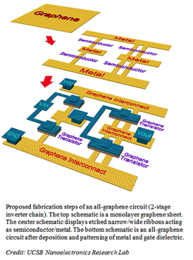
Santa Barbara, CA | Posted on October 23rd, 2013Bulk materials commonly used to make CMOS transitors and interconnects pose fundamental challenges in continuous shrinking of their feature-sizes and suffer from increasing "contact resistance" between them, both of which lead to degrading performance and rising energy consumption. Graphene-based transistors and interconnects are a promising nanoscale technology that could potentially address issues of traditional silicon-based transistors and metal interconnects.
"In addition to its atomically thin and pristine surfaces, graphene has a tunable band gap, which can be adjusted by lithographic sketching of patterns - narrow graphene ribbons can be made semiconducting while wider ribbons are metallic. Hence, contiguous graphene ribbons can be envisioned from the same starting material to design both active and passive devices in a seamless fashion and lower interface/contact resistances," explained Kaustav Banerjee, professor of electrical and computer engineering and director of the Nanoelectronics Research Lab at UCSB. Banerjee's research team also includes UCSB researchers Jiahao Kang, Deblina Sarkar and Yasin Khatami. Their work was recently published in the journal Applied Physics Letters.
"Accurate evaluation of electrical transport through the various graphene nanoribbon based devices and interconnects and across their interfaces was key to our successful circuit design and optimization," explained Jiahao Kang, a PhD student in Banerjee's group and a co-author of the study. Banerjee's group pioneered a methodology using the Non-Equilibrium Green's Function (NEGF) technique to evaluate the performance of such complex circuit schemes involving many heterojunctions. This methodology was used in designing an "all-graphene" logic circuit reported in this study.
"This work has demonstrated a solution for the serious contact resistance problem encounterd in conventional semiconductor technology by providing an innovative idea of using an all-graphene device-interconnect scheme. This will significantly simplify the IC fabrication process of graphene based nanoelectronic devices." commented Philip Kim, professor of physics at Columbia University, and a renowned scientist in the graphene world.
As reported in their study, the proposed all-graphene circuits have achieved 1.7X higher noise margins and 1-2 decades lower static power consumption over current CMOS technology. According to Banerjee, with the ongoing worldwide efforts in patterning and doping of graphene, such circuits can be realized in the near future.
"We hope that this work will encourage and inspire other researchers to explore graphene and beyond-graphene emerging 2-dimensional crystals for designing such �band-gap engineered' circuits in the near future," added Banerjee.
Their research was supported by the National Science Foundation.
####
About University of California - Santa Barbara
The College of Engineering at University of California, Santa Barbara is recognized globally as a leader among the top tier of engineering education and research programs, and is renowned for a successful interdisciplinary approach to engineering research.
For more information, please click here
Contacts:
Melissa Van De Werfhorst
Copyright © University of California - Santa Barbara
If you have a comment, please Contact us.Issuers of news releases, not 7th Wave, Inc. or Nanotechnology Now, are solely responsible for the accuracy of the content.
Bookmark:


| Related News Press |
News and information
![]() Quantum computer improves AI predictions April 17th, 2026
Quantum computer improves AI predictions April 17th, 2026
![]() Flexible sensor gains sensitivity under pressure April 17th, 2026
Flexible sensor gains sensitivity under pressure April 17th, 2026
![]() A reusable chip for particulate matter sensing April 17th, 2026
A reusable chip for particulate matter sensing April 17th, 2026
![]() Detecting vibrational quantum beating in the predissociation dynamics of SF6 using time-resolved photoelectron spectroscopy April 17th, 2026
Detecting vibrational quantum beating in the predissociation dynamics of SF6 using time-resolved photoelectron spectroscopy April 17th, 2026
Graphene/ Graphite
![]() Electrifying results shed light on graphene foam as a potential material for lab grown cartilage June 6th, 2025
Electrifying results shed light on graphene foam as a potential material for lab grown cartilage June 6th, 2025
![]() Breakthrough in proton barrier films using pore-free graphene oxide: Kumamoto University researchers achieve new milestone in advanced coating technologies September 13th, 2024
Breakthrough in proton barrier films using pore-free graphene oxide: Kumamoto University researchers achieve new milestone in advanced coating technologies September 13th, 2024
Govt.-Legislation/Regulation/Funding/Policy
![]() Quantum computer improves AI predictions April 17th, 2026
Quantum computer improves AI predictions April 17th, 2026
![]() Metasurfaces smooth light to boost magnetic sensing precision January 30th, 2026
Metasurfaces smooth light to boost magnetic sensing precision January 30th, 2026
![]() New imaging approach transforms study of bacterial biofilms August 8th, 2025
New imaging approach transforms study of bacterial biofilms August 8th, 2025
Chip Technology
![]() A reusable chip for particulate matter sensing April 17th, 2026
A reusable chip for particulate matter sensing April 17th, 2026
![]() Metasurfaces smooth light to boost magnetic sensing precision January 30th, 2026
Metasurfaces smooth light to boost magnetic sensing precision January 30th, 2026
Nanoelectronics
![]() Lab to industry: InSe wafer-scale breakthrough for future electronics August 8th, 2025
Lab to industry: InSe wafer-scale breakthrough for future electronics August 8th, 2025
![]() Interdisciplinary: Rice team tackles the future of semiconductors Multiferroics could be the key to ultralow-energy computing October 6th, 2023
Interdisciplinary: Rice team tackles the future of semiconductors Multiferroics could be the key to ultralow-energy computing October 6th, 2023
![]() Key element for a scalable quantum computer: Physicists from Forschungszentrum J�lich and RWTH Aachen University demonstrate electron transport on a quantum chip September 23rd, 2022
Key element for a scalable quantum computer: Physicists from Forschungszentrum J�lich and RWTH Aachen University demonstrate electron transport on a quantum chip September 23rd, 2022
![]() Reduced power consumption in semiconductor devices September 23rd, 2022
Reduced power consumption in semiconductor devices September 23rd, 2022
Discoveries
![]() Quantum computer improves AI predictions April 17th, 2026
Quantum computer improves AI predictions April 17th, 2026
![]() Flexible sensor gains sensitivity under pressure April 17th, 2026
Flexible sensor gains sensitivity under pressure April 17th, 2026
![]() A reusable chip for particulate matter sensing April 17th, 2026
A reusable chip for particulate matter sensing April 17th, 2026
![]() Detecting vibrational quantum beating in the predissociation dynamics of SF6 using time-resolved photoelectron spectroscopy April 17th, 2026
Detecting vibrational quantum beating in the predissociation dynamics of SF6 using time-resolved photoelectron spectroscopy April 17th, 2026
Announcements
![]() A fundamentally new therapeutic approach to cystic fibrosis: Nanobody repairs cellular defect April 17th, 2026
A fundamentally new therapeutic approach to cystic fibrosis: Nanobody repairs cellular defect April 17th, 2026
![]() UC Irvine physicists discover method to reverse �quantum scrambling� : The work addresses the problem of information loss in quantum computing system April 17th, 2026
UC Irvine physicists discover method to reverse �quantum scrambling� : The work addresses the problem of information loss in quantum computing system April 17th, 2026
Printing/Lithography/Inkjet/Inks/Bio-printing/Dyes
![]() Presenting: Ultrasound-based printing of 3D materials�potentially inside the body December 8th, 2023
Presenting: Ultrasound-based printing of 3D materials�potentially inside the body December 8th, 2023
![]() Simple ballpoint pen can write custom LEDs August 11th, 2023
Simple ballpoint pen can write custom LEDs August 11th, 2023
![]() Disposable electronics on a simple sheet of paper October 7th, 2022
Disposable electronics on a simple sheet of paper October 7th, 2022
|
|
||
|
|
||
| The latest news from around the world, FREE | ||
|
|
||
|
|
||
| Premium Products | ||
|
|
||
|
Only the news you want to read!
Learn More |
||
|
|
||
|
Full-service, expert consulting
Learn More |
||
|
|
||