Home > Press > Graphene on its way to conquer Silicon Valley
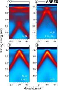 |
| These images were taken with the spectroscopy method ARPES while NiSi was formed under the graphene layer. In the final image (d) scientists can identify a particular spectrum (the linear Dirac-like spectrum of grapheme electrons) indicating that the graphene interacts only weakly with the metal silicides and therefore preserves its unique properties.
Credit: Vilkov et al., Sci. Rep. 2013, DOI: 10.1038/srep02168 |
Abstract:
The unique properties of graphene such as its incredible strength and, at the same time, its little weight have raised high expectations in modern material science. Graphene, a two-dimensional crystal of carbon atoms packed in a honeycomb structure, has been in the focus of intensive research which led to a Nobel Prize of Physics in 2010. One major challenge is to successfully integrate graphene into the established metal-silicide technology. Scientists from the University of Vienna and their co-workers from research institutes in Germany and Russia have succeeded in fabricating a novel structure of high-quality metal silicides all nicely covered and protected underneath a graphene layer. These two-dimensional sheets are as thin as single atoms.
Graphene on its way to conquer Silicon Valley
Vienna, Austria | Posted on July 9th, 2013Following Einstein's footsteps
In order to uncover the basic properties of the new structure the scientists need to resort to powerful measurement techniques based on one of Einstein's brilliant discoveries - the photoelectric effect. When a light particle interacts with a material it can transfer all its energy to an electron inside that material. If the energy of the light is sufficiently large, the electron acquires enough energy to escape from the material. Angle-resolved photoemission spectroscopy (ARPES) enables the scientists to extract valuable information on the electronic properties of the material by determining the angle under which the electrons escape from the material. "Single-atom thick layers and hybrid materials made thereof allow us to study a wealth of novel electronic phenomena and continue to fascinate the community of material scientists. The ARPES method plays a key role in these endeavours", say Alexander Grueneis and Nikolay Verbitskiy, members of the Electronic Properties of Materials Group at the University of Vienna and co-authors of the study.
Graphene keeping its head up high
The graphene-capped silicides under investigation are reliably protected against oxidation and can cover a wide range of electronic materials and device applications. Most importantly, the graphene layer itself barely interacts with the silicides underneath and the unique properties of graphene are widely preserved. The work of the research team, therefore, promises a clever way to incorporate graphene with existing metal silicide technology which finds a wide range of applications in semiconductor devices, spintronics, photovoltaics and thermoelectrics.
###
The work on graphene related materials is financed by a Marie Curie fellowship of the European commission and an APART fellowship of the Austrian Academy of Sciences.
Original publication:
"Controlled assembly of graphene-capped nickel, cobalt and iron silicides":
O. Vilkov, A. Fedorov, D. Usachov, L. V. Yashina, A. Generalov, K. Borygina, N. I. Verbitskiy, A. Grueneis, and D. V. Vyalikh
Scientific Reports, July 9, 2013,
DOI: 10.1038/srep02168
####
For more information, please click here
Contacts:
Dr. Alexander Grueneis
Electronic Properties of Materials
Faculty of Physics
University of Vienna
Boltzmanngasse 5, 1090 Vienna
M +43-664-602 77-513 72
Copyright © University of Vienna
If you have a comment, please Contact us.Issuers of news releases, not 7th Wave, Inc. or Nanotechnology Now, are solely responsible for the accuracy of the content.
Bookmark:


| Related Links |
![]() Dr. Alexander Grueneis homepage:
Dr. Alexander Grueneis homepage:
| Related News Press |
News and information
![]() Quantum computer improves AI predictions April 17th, 2026
Quantum computer improves AI predictions April 17th, 2026
![]() Flexible sensor gains sensitivity under pressure April 17th, 2026
Flexible sensor gains sensitivity under pressure April 17th, 2026
![]() A reusable chip for particulate matter sensing April 17th, 2026
A reusable chip for particulate matter sensing April 17th, 2026
![]() Detecting vibrational quantum beating in the predissociation dynamics of SF6 using time-resolved photoelectron spectroscopy April 17th, 2026
Detecting vibrational quantum beating in the predissociation dynamics of SF6 using time-resolved photoelectron spectroscopy April 17th, 2026
Graphene/ Graphite
![]() Electrifying results shed light on graphene foam as a potential material for lab grown cartilage June 6th, 2025
Electrifying results shed light on graphene foam as a potential material for lab grown cartilage June 6th, 2025
![]() Breakthrough in proton barrier films using pore-free graphene oxide: Kumamoto University researchers achieve new milestone in advanced coating technologies September 13th, 2024
Breakthrough in proton barrier films using pore-free graphene oxide: Kumamoto University researchers achieve new milestone in advanced coating technologies September 13th, 2024
Govt.-Legislation/Regulation/Funding/Policy
![]() Quantum computer improves AI predictions April 17th, 2026
Quantum computer improves AI predictions April 17th, 2026
![]() Metasurfaces smooth light to boost magnetic sensing precision January 30th, 2026
Metasurfaces smooth light to boost magnetic sensing precision January 30th, 2026
![]() New imaging approach transforms study of bacterial biofilms August 8th, 2025
New imaging approach transforms study of bacterial biofilms August 8th, 2025
Spintronics
![]() Quantum materials: Electron spin measured for the first time June 9th, 2023
Quantum materials: Electron spin measured for the first time June 9th, 2023
Chip Technology
![]() A reusable chip for particulate matter sensing April 17th, 2026
A reusable chip for particulate matter sensing April 17th, 2026
![]() Metasurfaces smooth light to boost magnetic sensing precision January 30th, 2026
Metasurfaces smooth light to boost magnetic sensing precision January 30th, 2026
Discoveries
![]() Quantum computer improves AI predictions April 17th, 2026
Quantum computer improves AI predictions April 17th, 2026
![]() Flexible sensor gains sensitivity under pressure April 17th, 2026
Flexible sensor gains sensitivity under pressure April 17th, 2026
![]() A reusable chip for particulate matter sensing April 17th, 2026
A reusable chip for particulate matter sensing April 17th, 2026
![]() Detecting vibrational quantum beating in the predissociation dynamics of SF6 using time-resolved photoelectron spectroscopy April 17th, 2026
Detecting vibrational quantum beating in the predissociation dynamics of SF6 using time-resolved photoelectron spectroscopy April 17th, 2026
Announcements
![]() A fundamentally new therapeutic approach to cystic fibrosis: Nanobody repairs cellular defect April 17th, 2026
A fundamentally new therapeutic approach to cystic fibrosis: Nanobody repairs cellular defect April 17th, 2026
![]() UC Irvine physicists discover method to reverse �quantum scrambling� : The work addresses the problem of information loss in quantum computing system April 17th, 2026
UC Irvine physicists discover method to reverse �quantum scrambling� : The work addresses the problem of information loss in quantum computing system April 17th, 2026
Interviews/Book Reviews/Essays/Reports/Podcasts/Journals/White papers/Posters
![]() A fundamentally new therapeutic approach to cystic fibrosis: Nanobody repairs cellular defect April 17th, 2026
A fundamentally new therapeutic approach to cystic fibrosis: Nanobody repairs cellular defect April 17th, 2026
![]() UC Irvine physicists discover method to reverse �quantum scrambling� : The work addresses the problem of information loss in quantum computing system April 17th, 2026
UC Irvine physicists discover method to reverse �quantum scrambling� : The work addresses the problem of information loss in quantum computing system April 17th, 2026
Energy
![]() Sensors innovations for smart lithium-based batteries: advancements, opportunities, and potential challenges August 8th, 2025
Sensors innovations for smart lithium-based batteries: advancements, opportunities, and potential challenges August 8th, 2025
![]() Simple algorithm paired with standard imaging tool could predict failure in lithium metal batteries August 8th, 2025
Simple algorithm paired with standard imaging tool could predict failure in lithium metal batteries August 8th, 2025
Grants/Sponsored Research/Awards/Scholarships/Gifts/Contests/Honors/Records
![]() Quantum computer improves AI predictions April 17th, 2026
Quantum computer improves AI predictions April 17th, 2026
![]() Detecting vibrational quantum beating in the predissociation dynamics of SF6 using time-resolved photoelectron spectroscopy April 17th, 2026
Detecting vibrational quantum beating in the predissociation dynamics of SF6 using time-resolved photoelectron spectroscopy April 17th, 2026
![]() Metasurfaces smooth light to boost magnetic sensing precision January 30th, 2026
Metasurfaces smooth light to boost magnetic sensing precision January 30th, 2026
Solar/Photovoltaic
![]() Spinel-type sulfide semiconductors to operate the next-generation LEDs and solar cells For solar-cell absorbers and green-LED source October 3rd, 2025
Spinel-type sulfide semiconductors to operate the next-generation LEDs and solar cells For solar-cell absorbers and green-LED source October 3rd, 2025
![]() KAIST researchers introduce new and improved, next-generation perovskite solar cell November 8th, 2024
KAIST researchers introduce new and improved, next-generation perovskite solar cell November 8th, 2024
![]() Groundbreaking precision in single-molecule optoelectronics August 16th, 2024
Groundbreaking precision in single-molecule optoelectronics August 16th, 2024
![]() Development of zinc oxide nanopagoda array photoelectrode: photoelectrochemical water-splitting hydrogen production January 12th, 2024
Development of zinc oxide nanopagoda array photoelectrode: photoelectrochemical water-splitting hydrogen production January 12th, 2024
|
|
||
|
|
||
| The latest news from around the world, FREE | ||
|
|
||
|
|
||
| Premium Products | ||
|
|
||
|
Only the news you want to read!
Learn More |
||
|
|
||
|
Full-service, expert consulting
Learn More |
||
|
|
||