Home > Press > Samsung funding is awarded for development of novel nano-magnetic device architectures
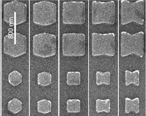 |
| Electron micrograph of nanofabricated magnetic nanostructures, where the magnetic properties are controlled via the structure's geometry and size. |
Abstract:
Dr Colm Durkan, currently the head of Cambridge University's Nanoscience Research Group, has been awarded funding from the Samsung Global Research Outreach (GRO) programme, for research and development of novel magnetic devices for information processing. This was a highly competitive funding round with only 23 grants awarded worldwide.
Samsung funding is awarded for development of novel nano-magnetic device architectures
UK | Posted on December 13th, 2010The world of electronics has reached a junction whereby new paradigms are continually emerging. Transistors fabricated using conventional processes are already small enough (~ 20 nm) that they are on the verge of demonstrating quantum effects involving tunneling, localization and electron interference. One of the most promising avenues however, is spintronics, where the spin degree of freedom of the electron to do something novel is utilized.
Colm and his team are interested in the fundamentals underpinning some of this technology. Colm says; 'There is a large scientific community investigating novel materials for data storage, whereas our interest is in the size effect of soft magnetic materials in general. Our expertise is specifically in the fabrication and functional characterization of nanostructures by scanning probe microscopy, combined with state-of-the art modelling.'
Colm has already pioneered several scanning probe microscopy developments in the field, work that led to election to a fellowship of the Institute of Physics earlier this year and promotion to a personal readership in October 2010.
'For magnetic structures with dimensions below around 1�m, the magnetic properties are determined to a large extent by the geometry and size of the structures. On the more extreme scale of ultra-thin films of magnetic materials, it has recently been shown that one may dramatically alter magnetic properties simply by controlling film thickness and substrate surface. Therefore, we wish to tap into this treasure chest of nanomagnetism to realize novel data storage, information processing and spin readout systems to increase the functionality of electronic components without significant cost implications.'
Some of Colm's recent work on this topic has recently been published in Physical Review B.
Webpage: www.eng.cam.ac.uk/~cd229/
####
For more information, please click here
Contacts:
Dr Colm Durkan
www.eng.cam.ac.uk/~cd229/
Copyright © Cambridge University
If you have a comment, please Contact us.Issuers of news releases, not 7th Wave, Inc. or Nanotechnology Now, are solely responsible for the accuracy of the content.
Bookmark:


| Related News Press |
News and information
![]() Quantum computer improves AI predictions April 17th, 2026
Quantum computer improves AI predictions April 17th, 2026
![]() Flexible sensor gains sensitivity under pressure April 17th, 2026
Flexible sensor gains sensitivity under pressure April 17th, 2026
![]() A reusable chip for particulate matter sensing April 17th, 2026
A reusable chip for particulate matter sensing April 17th, 2026
![]() Detecting vibrational quantum beating in the predissociation dynamics of SF6 using time-resolved photoelectron spectroscopy April 17th, 2026
Detecting vibrational quantum beating in the predissociation dynamics of SF6 using time-resolved photoelectron spectroscopy April 17th, 2026
Govt.-Legislation/Regulation/Funding/Policy
![]() Quantum computer improves AI predictions April 17th, 2026
Quantum computer improves AI predictions April 17th, 2026
![]() Metasurfaces smooth light to boost magnetic sensing precision January 30th, 2026
Metasurfaces smooth light to boost magnetic sensing precision January 30th, 2026
![]() New imaging approach transforms study of bacterial biofilms August 8th, 2025
New imaging approach transforms study of bacterial biofilms August 8th, 2025
Possible Futures
![]() A fundamentally new therapeutic approach to cystic fibrosis: Nanobody repairs cellular defect April 17th, 2026
A fundamentally new therapeutic approach to cystic fibrosis: Nanobody repairs cellular defect April 17th, 2026
![]() UC Irvine physicists discover method to reverse �quantum scrambling� : The work addresses the problem of information loss in quantum computing system April 17th, 2026
UC Irvine physicists discover method to reverse �quantum scrambling� : The work addresses the problem of information loss in quantum computing system April 17th, 2026
Academic/Education
![]() Rice University launches Rice Synthetic Biology Institute to improve lives January 12th, 2024
Rice University launches Rice Synthetic Biology Institute to improve lives January 12th, 2024
![]() Multi-institution, $4.6 million NSF grant to fund nanotechnology training September 9th, 2022
Multi-institution, $4.6 million NSF grant to fund nanotechnology training September 9th, 2022
Spintronics
![]() Quantum materials: Electron spin measured for the first time June 9th, 2023
Quantum materials: Electron spin measured for the first time June 9th, 2023
Chip Technology
![]() A reusable chip for particulate matter sensing April 17th, 2026
A reusable chip for particulate matter sensing April 17th, 2026
![]() Metasurfaces smooth light to boost magnetic sensing precision January 30th, 2026
Metasurfaces smooth light to boost magnetic sensing precision January 30th, 2026
Nanoelectronics
![]() Lab to industry: InSe wafer-scale breakthrough for future electronics August 8th, 2025
Lab to industry: InSe wafer-scale breakthrough for future electronics August 8th, 2025
![]() Interdisciplinary: Rice team tackles the future of semiconductors Multiferroics could be the key to ultralow-energy computing October 6th, 2023
Interdisciplinary: Rice team tackles the future of semiconductors Multiferroics could be the key to ultralow-energy computing October 6th, 2023
![]() Key element for a scalable quantum computer: Physicists from Forschungszentrum J�lich and RWTH Aachen University demonstrate electron transport on a quantum chip September 23rd, 2022
Key element for a scalable quantum computer: Physicists from Forschungszentrum J�lich and RWTH Aachen University demonstrate electron transport on a quantum chip September 23rd, 2022
![]() Reduced power consumption in semiconductor devices September 23rd, 2022
Reduced power consumption in semiconductor devices September 23rd, 2022
Announcements
![]() A fundamentally new therapeutic approach to cystic fibrosis: Nanobody repairs cellular defect April 17th, 2026
A fundamentally new therapeutic approach to cystic fibrosis: Nanobody repairs cellular defect April 17th, 2026
![]() UC Irvine physicists discover method to reverse �quantum scrambling� : The work addresses the problem of information loss in quantum computing system April 17th, 2026
UC Irvine physicists discover method to reverse �quantum scrambling� : The work addresses the problem of information loss in quantum computing system April 17th, 2026
|
|
||
|
|
||
| The latest news from around the world, FREE | ||
|
|
||
|
|
||
| Premium Products | ||
|
|
||
|
Only the news you want to read!
Learn More |
||
|
|
||
|
Full-service, expert consulting
Learn More |
||
|
|
||