Home > Press > Laboratory record: new chip platform increases LED efficiency by 30%
 |
| The 30% increase in the efficiency of the diode results from improved material properties, further development of the thin-film platform and greater output efficiency � and unencapsulated chips benefit even more from the improvements. (Press picture: OSRAM) |
Abstract:
Prototype of a red Golden Dragon Plus LED sets new record
Laboratory record: new chip platform increases LED efficiency by 30%
Regensburg, Germany | Posted on July 24th, 2010Developers at OSRAM Opto Semiconductors have succeeded in increasing the efficiency of red thin-film LEDs by 30% - a new record. The latest generation of thin-film chips benefit from an optimized chip platform which has potential for further improvements. This boost in efficiency is opening up new LED applications in general illumination, in projection and in the industrial sector.
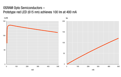
The record efficiency for an LED of 119 lm/W at an operating current of 350 mA (136 lm/W at 70mA) has been achieved by the latest generation of a red 1 mm� thin-film chip (InGaAlP). The chip is accommodated in a Golden Dragon Plus package and emits at a wavelength of 615 nm (� dominant). At present there is no LED with higher efficiency at this wavelength. Its efficiency has been measured at 44% (49% at 70mA), and even exceeds 50% for a wavelength of 642 nm.
Higher efficiency means greater output for the same current and lower power consumption in the relevant applications. There are also new design options because fewer chips will be needed and therefore less space to produce the same brightness. In addition, almost 50% less waste heat needs to be removed, which in turn considerably reduces the need for cooling. As brightness increases, the light sources can be made smaller and smaller.
The improved performance of the LEDs greatly expands the possible applications for this innovative light source. For example, exceptionally high efficiency means that warm white LED solutions can be produced with better quality of light and a better energy balance through color mixing than through the usual conversion of blue light.
"This will benefit all applications that use high-efficiency red, particularly projection applications. We expect to start equipping LED products with the new thin-film chips in about a year's time," said Dr. Wolfgang Schmid, who is responsible for developing this chip technology at OSRAM Opto Semiconductors.
####
About OSRAM
OSRAM is part of the Industry sector of Siemens and one of the two leading lighting manufacturers in the world. Its subsidiary, OSRAM Opto Semiconductors GmbH in Regensburg (Germany), offers its customers solutions based on semiconductor technology for lighting, sensor and visualization applications. OSRAM Opto Semiconductors has production sites in Regensburg (Germany) and Penang (Malaysia). Its headquarters for North America is in Sunnyvale (USA), and for Asia in Hong Kong. OSRAM Opto Semiconductors also has sales offices throughout the world. For more information go to www.osram-os.com.
For more information, please click here
Contacts:
Mrs. Marion Reichl
Osram GmbH
Tel: +49 (941) 850 1693
Copyright © OSRAM
If you have a comment, please Contact us.Issuers of news releases, not 7th Wave, Inc. or Nanotechnology Now, are solely responsible for the accuracy of the content.
Bookmark:


| Related News Press |
News and information
![]() Quantum computer improves AI predictions April 17th, 2026
Quantum computer improves AI predictions April 17th, 2026
![]() Flexible sensor gains sensitivity under pressure April 17th, 2026
Flexible sensor gains sensitivity under pressure April 17th, 2026
![]() A reusable chip for particulate matter sensing April 17th, 2026
A reusable chip for particulate matter sensing April 17th, 2026
![]() Detecting vibrational quantum beating in the predissociation dynamics of SF6 using time-resolved photoelectron spectroscopy April 17th, 2026
Detecting vibrational quantum beating in the predissociation dynamics of SF6 using time-resolved photoelectron spectroscopy April 17th, 2026
Thin films
![]() Tiny nanosheets, big leap: A new sensor detects ethanol at ultra-low levels January 30th, 2026
Tiny nanosheets, big leap: A new sensor detects ethanol at ultra-low levels January 30th, 2026
Display technology/LEDs/SS Lighting/OLEDs
![]() Spinel-type sulfide semiconductors to operate the next-generation LEDs and solar cells For solar-cell absorbers and green-LED source October 3rd, 2025
Spinel-type sulfide semiconductors to operate the next-generation LEDs and solar cells For solar-cell absorbers and green-LED source October 3rd, 2025
![]() Efficient and stable hybrid perovskite-organic light-emitting diodes with external quantum efficiency exceeding 40 per cent July 5th, 2024
Efficient and stable hybrid perovskite-organic light-emitting diodes with external quantum efficiency exceeding 40 per cent July 5th, 2024
Possible Futures
![]() A fundamentally new therapeutic approach to cystic fibrosis: Nanobody repairs cellular defect April 17th, 2026
A fundamentally new therapeutic approach to cystic fibrosis: Nanobody repairs cellular defect April 17th, 2026
![]() UC Irvine physicists discover method to reverse �quantum scrambling� : The work addresses the problem of information loss in quantum computing system April 17th, 2026
UC Irvine physicists discover method to reverse �quantum scrambling� : The work addresses the problem of information loss in quantum computing system April 17th, 2026
Nanoelectronics
![]() Lab to industry: InSe wafer-scale breakthrough for future electronics August 8th, 2025
Lab to industry: InSe wafer-scale breakthrough for future electronics August 8th, 2025
![]() Interdisciplinary: Rice team tackles the future of semiconductors Multiferroics could be the key to ultralow-energy computing October 6th, 2023
Interdisciplinary: Rice team tackles the future of semiconductors Multiferroics could be the key to ultralow-energy computing October 6th, 2023
![]() Key element for a scalable quantum computer: Physicists from Forschungszentrum J�lich and RWTH Aachen University demonstrate electron transport on a quantum chip September 23rd, 2022
Key element for a scalable quantum computer: Physicists from Forschungszentrum J�lich and RWTH Aachen University demonstrate electron transport on a quantum chip September 23rd, 2022
![]() Reduced power consumption in semiconductor devices September 23rd, 2022
Reduced power consumption in semiconductor devices September 23rd, 2022
Announcements
![]() A fundamentally new therapeutic approach to cystic fibrosis: Nanobody repairs cellular defect April 17th, 2026
A fundamentally new therapeutic approach to cystic fibrosis: Nanobody repairs cellular defect April 17th, 2026
![]() UC Irvine physicists discover method to reverse �quantum scrambling� : The work addresses the problem of information loss in quantum computing system April 17th, 2026
UC Irvine physicists discover method to reverse �quantum scrambling� : The work addresses the problem of information loss in quantum computing system April 17th, 2026
|
|
||
|
|
||
| The latest news from around the world, FREE | ||
|
|
||
|
|
||
| Premium Products | ||
|
|
||
|
Only the news you want to read!
Learn More |
||
|
|
||
|
Full-service, expert consulting
Learn More |
||
|
|
||