Home > Press > MIT uses nano-origami to build tiny electronic devices
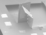 |
| MIT researchers have developed a way to fold nano- and microscale polymer sheets into simple 3D structures. |
Abstract:
Folding paper into shapes such as a crane or a butterfly is challenging enough for most people. Now imagine trying to fold something that's about a hundred times thinner than a human hair and then putting it to use as an electronic device.
MIT uses nano-origami to build tiny electronic devices
Cambridge, MA | Posted on February 26th, 2009A team of researchers led by George Barbastathis, associate professor of mechanical engineering, is developing the basic principles of nano-origami, a new technique that allows engineers to fold nanoscale materials into simple 3-D structures. The tiny folded materials could be used as motors and capacitors, potentially leading to better computer memory storage, faster microprocessors and new nanophotonic devices.
Traditional micro- and nano-fabrication techniques such as X-ray lithography and nano-imprinting work beautifully for two-dimensional structures, and are commonly used to build microprocessors and other micro-electrical-mechanical (MEMS) devices. However, they cannot create 3-D structures.
"A lot of what's done now is planar," says Tony Nichol, a mechanical engineering graduate student working on the project. "We want to take all of the nice tools that have been developed for 2-D and do 3-D things."
The MIT team uses conventional lithography tools to pattern 2-D materials at the nanoscale, then folds them into predetermined 3-D shapes, opening a new realm of possible applications.
Smaller, faster
The researchers have already demonstrated a 3-D nanoscale capacitor, developed in collaboration with MIT Professor Yang Shao-Horn, which was presented at the 2005 meeting of the Electrochemical Society. The current model has only one fold but the more folds that are added, the more energy it will be able to store. Extra layers also promote faster information flow, just as the human brain's many folds allow for quicker communication between brain regions, says Nader Shaar, a mechanical engineering graduate student working on the project.
Getting the materials to fold back and forth into an accordion-like structure has been one of the researchers' biggest challenges, along with getting the faces and edges to line up accurately.
They have worked out several ways to induce the nanomaterials to fold, including:
* Depositing metal (usually chromium) onto the surface where you want the fold to be. This causes the material to curl upward, but it does not allow for right angles or accordion-type folds.
* Directing a beam of helium ions onto the desired fold location. The beams imprint patterns that will cause the material to fold once it's removed from the surface. High-energy beams go to the bottom of the material and cause it to fold up; ions from low-energy beams accumulate at the top of the material and make it fold down.
* Embedding gold wires in the material. A current running along the gold wires interacts with an external magnetic field, creating a Lorentz force that lifts the face. This technique is a form of directed self-assembly, where the designer provides the template and then lets the device assemble itself.
The folded shapes can be fabricated with a few different types of material, including silicon, silicon nitride (a type of ceramic) and a soft polymer known as SU-8.
Once the material is folded, the tricky part is getting the faces to align properly. The researchers have developed a few ways to do this successfully: one uses magnets; another involves attaching polymers to a certain spot on the faces and melting them with an electric current, sealing the two faces together.
They're still working on getting faces and edges of a folded cube to line up with nanoscale precision, but Shaar, co-supervised by associate professor of mechanical engineering Carol Livermore, has devised a promising method that uses three pairs of matching holes and protrusions to pull the edge and face into alignment.
The researchers are deep in the development phase of their nano-folded devices, but they are starting to think about how the technology could be used in the future. "We've got the core components figured out, and now we're just having fun with figuring out some applications," says Nichol.
Written by Anne Trafton, MIT News Office
####
For more information, please click here
Contacts:
Elizabeth A. Thomson
MIT News Office
T: 617-258-5402
Copyright © MIT
If you have a comment, please Contact us.Issuers of news releases, not 7th Wave, Inc. or Nanotechnology Now, are solely responsible for the accuracy of the content.
Bookmark:


| Related Links |
| Related News Press |
News and information
![]() Quantum computer improves AI predictions April 17th, 2026
Quantum computer improves AI predictions April 17th, 2026
![]() Flexible sensor gains sensitivity under pressure April 17th, 2026
Flexible sensor gains sensitivity under pressure April 17th, 2026
![]() A reusable chip for particulate matter sensing April 17th, 2026
A reusable chip for particulate matter sensing April 17th, 2026
![]() Detecting vibrational quantum beating in the predissociation dynamics of SF6 using time-resolved photoelectron spectroscopy April 17th, 2026
Detecting vibrational quantum beating in the predissociation dynamics of SF6 using time-resolved photoelectron spectroscopy April 17th, 2026
Videos/Movies
![]() ICFO researchers overcome long-standing bottleneck in single photon detection with twisted 2D materials August 8th, 2025
ICFO researchers overcome long-standing bottleneck in single photon detection with twisted 2D materials August 8th, 2025
![]() New X-ray imaging technique to study the transient phases of quantum materials December 29th, 2022
New X-ray imaging technique to study the transient phases of quantum materials December 29th, 2022
![]() Solvent study solves solar cell durability puzzle: Rice-led project could make perovskite cells ready for prime time September 23rd, 2022
Solvent study solves solar cell durability puzzle: Rice-led project could make perovskite cells ready for prime time September 23rd, 2022
![]() Scientists prepare for the world�s smallest race: Nanocar Race II March 18th, 2022
Scientists prepare for the world�s smallest race: Nanocar Race II March 18th, 2022
Chip Technology
![]() A reusable chip for particulate matter sensing April 17th, 2026
A reusable chip for particulate matter sensing April 17th, 2026
![]() Metasurfaces smooth light to boost magnetic sensing precision January 30th, 2026
Metasurfaces smooth light to boost magnetic sensing precision January 30th, 2026
Memory Technology
![]() Researchers tackle the memory bottleneck stalling quantum computing October 3rd, 2025
Researchers tackle the memory bottleneck stalling quantum computing October 3rd, 2025
![]() First real-time observation of two-dimensional melting process: Researchers at Mainz University unveil new insights into magnetic vortex structures August 8th, 2025
First real-time observation of two-dimensional melting process: Researchers at Mainz University unveil new insights into magnetic vortex structures August 8th, 2025
![]() Utilizing palladium for addressing contact issues of buried oxide thin film transistors April 5th, 2024
Utilizing palladium for addressing contact issues of buried oxide thin film transistors April 5th, 2024
Nanoelectronics
![]() Lab to industry: InSe wafer-scale breakthrough for future electronics August 8th, 2025
Lab to industry: InSe wafer-scale breakthrough for future electronics August 8th, 2025
![]() Interdisciplinary: Rice team tackles the future of semiconductors Multiferroics could be the key to ultralow-energy computing October 6th, 2023
Interdisciplinary: Rice team tackles the future of semiconductors Multiferroics could be the key to ultralow-energy computing October 6th, 2023
![]() Key element for a scalable quantum computer: Physicists from Forschungszentrum J�lich and RWTH Aachen University demonstrate electron transport on a quantum chip September 23rd, 2022
Key element for a scalable quantum computer: Physicists from Forschungszentrum J�lich and RWTH Aachen University demonstrate electron transport on a quantum chip September 23rd, 2022
![]() Reduced power consumption in semiconductor devices September 23rd, 2022
Reduced power consumption in semiconductor devices September 23rd, 2022
Discoveries
![]() Quantum computer improves AI predictions April 17th, 2026
Quantum computer improves AI predictions April 17th, 2026
![]() Flexible sensor gains sensitivity under pressure April 17th, 2026
Flexible sensor gains sensitivity under pressure April 17th, 2026
![]() A reusable chip for particulate matter sensing April 17th, 2026
A reusable chip for particulate matter sensing April 17th, 2026
![]() Detecting vibrational quantum beating in the predissociation dynamics of SF6 using time-resolved photoelectron spectroscopy April 17th, 2026
Detecting vibrational quantum beating in the predissociation dynamics of SF6 using time-resolved photoelectron spectroscopy April 17th, 2026
Announcements
![]() A fundamentally new therapeutic approach to cystic fibrosis: Nanobody repairs cellular defect April 17th, 2026
A fundamentally new therapeutic approach to cystic fibrosis: Nanobody repairs cellular defect April 17th, 2026
![]() UC Irvine physicists discover method to reverse �quantum scrambling� : The work addresses the problem of information loss in quantum computing system April 17th, 2026
UC Irvine physicists discover method to reverse �quantum scrambling� : The work addresses the problem of information loss in quantum computing system April 17th, 2026
Photonics/Optics/Lasers
![]() Metasurfaces smooth light to boost magnetic sensing precision January 30th, 2026
Metasurfaces smooth light to boost magnetic sensing precision January 30th, 2026
![]() From sensors to smart systems: the rise of AI-driven photonic noses January 30th, 2026
From sensors to smart systems: the rise of AI-driven photonic noses January 30th, 2026
|
|
||
|
|
||
| The latest news from around the world, FREE | ||
|
|
||
|
|
||
| Premium Products | ||
|
|
||
|
Only the news you want to read!
Learn More |
||
|
|
||
|
Full-service, expert consulting
Learn More |
||
|
|
||