Home > Press > Printed perovskite LEDs: An innovative technique towards a new standard process of electronics manufacturing
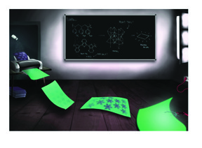 |
| Graphic representation of the printing process for the perovskite LED. � Claudia Rothkirch/HU Berlin |
Abstract:
Microelectronics utilise various functional materials whose properties make them suitable for specific applications. For example, transistors and data storage devices are made of silicon, and most photovoltaic cells used for generating electricity from sunlight are also currently made of this semiconductor material. In contrast, compound semiconductors such as gallium nitride are used to generate light in optoelectronic elements such as light-emitting diodes (LEDs). The manufacturing processes also different for the various classes of materials.
Printed perovskite LEDs: An innovative technique towards a new standard process of electronics manufacturing
Berlin, Germany | Posted on June 12th, 2020Transcending the materials and methods maze
Hybrid perovskite materials promise simplification - by arranging the organic and inorganic components of semiconducting crystal in a specific structure. "They can be used to manufacture all kinds of microelectronic components by modifying their composition", says Prof. Emil List-Kratochvil, head of a Joint Research Group at HZB and Humboldt-Universit�t.
What's more, processing perovskite crystals is comparatively simple. "They can be produced from a liquid solution, so you can build the desired component one layer at a time directly on the substrate", the physicist explains.
First solar cells from an inkjet printer, now light-emitting diodes too
Scientists at HZB have already shown in recent years that solar cells can be printed from a solution of semiconductor compounds - and are worldwide leaders in this technology today. Now for the first time, the joint team of HZB and HU Berlin has succeeded in producing functional light-emitting diodes in this manner. The research group used a metal halide perovskite for this purpose. This is a material that promises particularly high efficiency in generating light - but on the other hand is difficult to process.
"Until now, it has not been possible to produce these kinds of semiconductor layers with sufficient quality from a liquid solution", says List-Kratochvil. For example, LEDs could be printed just from organic semiconductors, but these provide only modest luminosity. "The challenge was how to cause the salt-like precursor that we printed onto the substrate to crystallise quickly and evenly by using some sort of an attractant or catalyst", explains the scientist. The team chose a seed crystal for this purpose: a salt crystal that attaches itself to the substrate and triggers formation of a gridwork for the subsequent perovskite layers.
Significantly better optical and electronic characteristics
In this way, the researchers created printed LEDs that possess far higher luminosity and considerably better electrical properties than could be previously achieved using additive manufacturing processes. But for List-Kratochvil, this success is only an intermediate step on the road to future micro- and optoelectronics that he believes will be based exclusively on hybrid perovskite semiconductors. "The advantages offered by a single universally applicable class of materials and a single cost-effective and simple process for manufacturing any kind of component are striking", says the scientist. He is therefore planning to eventually manufacture all important electronic components this way in the laboratories of HZB and HU Berlin.
List-Kratochvil is Professor of Hybrid Devices at the Humboldt-Universit�t zu Berlin and head of a Joint Lab founded in 2018 that is operated by HU together with HZB. In addition, a team jointly headed by List-Kratochvil and HZB scientist Dr. Eva Unger is working in the Helmholtz Innovation Lab HySPRINT on the development of coating and printing processes - also known in technical jargon as "additive manufacturing" - for hybrid perovskites. These are crystals possessing a perovskite structure that contain both inorganic and organic components.
###
The work was published in Materials Horizons, the journal of the Royal Society of Chemistry, in an article entitled "Finally, inkjet-printed metal-halide perovskite LEDs - utilizing seed-crystal templating of salty PEDOT:PSS" by Felix Hermerschmidt, Florian Mathies, Vincent R. F. Schr�der, Carolin Rehermann, Nicolas Zorn Morales, Eva L. Unger, Emil J. W. List-Kratochvil.
####
For more information, please click here
Contacts:
Emil List-Kratochvil
49-302-093-7697
@HZBde
Copyright © Helmholtz-Zentrum Berlin f�r Materialien und Energie
If you have a comment, please Contact us.Issuers of news releases, not 7th Wave, Inc. or Nanotechnology Now, are solely responsible for the accuracy of the content.
Bookmark:


| Related Links |
| Related News Press |
News and information
![]() Quantum computer improves AI predictions April 17th, 2026
Quantum computer improves AI predictions April 17th, 2026
![]() Flexible sensor gains sensitivity under pressure April 17th, 2026
Flexible sensor gains sensitivity under pressure April 17th, 2026
![]() A reusable chip for particulate matter sensing April 17th, 2026
A reusable chip for particulate matter sensing April 17th, 2026
![]() Detecting vibrational quantum beating in the predissociation dynamics of SF6 using time-resolved photoelectron spectroscopy April 17th, 2026
Detecting vibrational quantum beating in the predissociation dynamics of SF6 using time-resolved photoelectron spectroscopy April 17th, 2026
Display technology/LEDs/SS Lighting/OLEDs
![]() Spinel-type sulfide semiconductors to operate the next-generation LEDs and solar cells For solar-cell absorbers and green-LED source October 3rd, 2025
Spinel-type sulfide semiconductors to operate the next-generation LEDs and solar cells For solar-cell absorbers and green-LED source October 3rd, 2025
Perovskites
![]() KAIST researchers introduce new and improved, next-generation perovskite solar cell November 8th, 2024
KAIST researchers introduce new and improved, next-generation perovskite solar cell November 8th, 2024
3D & 4D printing/Additive-manufacturing
![]() Presenting: Ultrasound-based printing of 3D materials�potentially inside the body December 8th, 2023
Presenting: Ultrasound-based printing of 3D materials�potentially inside the body December 8th, 2023
![]() Fiber sensing scientists invent 3D printed fiber microprobe for measuring in vivo biomechanical properties of tissue and even single cell February 10th, 2023
Fiber sensing scientists invent 3D printed fiber microprobe for measuring in vivo biomechanical properties of tissue and even single cell February 10th, 2023
![]() 3D-printed decoder, AI-enabled image compression could enable higher-res displays December 9th, 2022
3D-printed decoder, AI-enabled image compression could enable higher-res displays December 9th, 2022
![]() Researchers design new inks for 3D-printable wearable bioelectronics: Potential uses include printing electronic tattoos for medical tracking applications August 19th, 2022
Researchers design new inks for 3D-printable wearable bioelectronics: Potential uses include printing electronic tattoos for medical tracking applications August 19th, 2022
Possible Futures
![]() A fundamentally new therapeutic approach to cystic fibrosis: Nanobody repairs cellular defect April 17th, 2026
A fundamentally new therapeutic approach to cystic fibrosis: Nanobody repairs cellular defect April 17th, 2026
![]() UC Irvine physicists discover method to reverse �quantum scrambling� : The work addresses the problem of information loss in quantum computing system April 17th, 2026
UC Irvine physicists discover method to reverse �quantum scrambling� : The work addresses the problem of information loss in quantum computing system April 17th, 2026
Chip Technology
![]() A reusable chip for particulate matter sensing April 17th, 2026
A reusable chip for particulate matter sensing April 17th, 2026
![]() Metasurfaces smooth light to boost magnetic sensing precision January 30th, 2026
Metasurfaces smooth light to boost magnetic sensing precision January 30th, 2026
Optical computing/Photonic computing
![]() ICFO researchers overcome long-standing bottleneck in single photon detection with twisted 2D materials August 8th, 2025
ICFO researchers overcome long-standing bottleneck in single photon detection with twisted 2D materials August 8th, 2025
![]() Programmable electron-induced color router array May 14th, 2025
Programmable electron-induced color router array May 14th, 2025
Discoveries
![]() Quantum computer improves AI predictions April 17th, 2026
Quantum computer improves AI predictions April 17th, 2026
![]() Flexible sensor gains sensitivity under pressure April 17th, 2026
Flexible sensor gains sensitivity under pressure April 17th, 2026
![]() A reusable chip for particulate matter sensing April 17th, 2026
A reusable chip for particulate matter sensing April 17th, 2026
![]() Detecting vibrational quantum beating in the predissociation dynamics of SF6 using time-resolved photoelectron spectroscopy April 17th, 2026
Detecting vibrational quantum beating in the predissociation dynamics of SF6 using time-resolved photoelectron spectroscopy April 17th, 2026
Materials/Metamaterials/Magnetoresistance
![]() First real-time observation of two-dimensional melting process: Researchers at Mainz University unveil new insights into magnetic vortex structures August 8th, 2025
First real-time observation of two-dimensional melting process: Researchers at Mainz University unveil new insights into magnetic vortex structures August 8th, 2025
![]() Researchers unveil a groundbreaking clay-based solution to capture carbon dioxide and combat climate change June 6th, 2025
Researchers unveil a groundbreaking clay-based solution to capture carbon dioxide and combat climate change June 6th, 2025
![]() A 1960s idea inspires NBI researchers to study hitherto inaccessible quantum states June 6th, 2025
A 1960s idea inspires NBI researchers to study hitherto inaccessible quantum states June 6th, 2025
![]() Institute for Nanoscience hosts annual proposal planning meeting May 16th, 2025
Institute for Nanoscience hosts annual proposal planning meeting May 16th, 2025
Announcements
![]() A fundamentally new therapeutic approach to cystic fibrosis: Nanobody repairs cellular defect April 17th, 2026
A fundamentally new therapeutic approach to cystic fibrosis: Nanobody repairs cellular defect April 17th, 2026
![]() UC Irvine physicists discover method to reverse �quantum scrambling� : The work addresses the problem of information loss in quantum computing system April 17th, 2026
UC Irvine physicists discover method to reverse �quantum scrambling� : The work addresses the problem of information loss in quantum computing system April 17th, 2026
Interviews/Book Reviews/Essays/Reports/Podcasts/Journals/White papers/Posters
![]() A fundamentally new therapeutic approach to cystic fibrosis: Nanobody repairs cellular defect April 17th, 2026
A fundamentally new therapeutic approach to cystic fibrosis: Nanobody repairs cellular defect April 17th, 2026
![]() UC Irvine physicists discover method to reverse �quantum scrambling� : The work addresses the problem of information loss in quantum computing system April 17th, 2026
UC Irvine physicists discover method to reverse �quantum scrambling� : The work addresses the problem of information loss in quantum computing system April 17th, 2026
Solar/Photovoltaic
![]() Spinel-type sulfide semiconductors to operate the next-generation LEDs and solar cells For solar-cell absorbers and green-LED source October 3rd, 2025
Spinel-type sulfide semiconductors to operate the next-generation LEDs and solar cells For solar-cell absorbers and green-LED source October 3rd, 2025
![]() KAIST researchers introduce new and improved, next-generation perovskite solar cell November 8th, 2024
KAIST researchers introduce new and improved, next-generation perovskite solar cell November 8th, 2024
![]() Groundbreaking precision in single-molecule optoelectronics August 16th, 2024
Groundbreaking precision in single-molecule optoelectronics August 16th, 2024
![]() Development of zinc oxide nanopagoda array photoelectrode: photoelectrochemical water-splitting hydrogen production January 12th, 2024
Development of zinc oxide nanopagoda array photoelectrode: photoelectrochemical water-splitting hydrogen production January 12th, 2024
Printing/Lithography/Inkjet/Inks/Bio-printing/Dyes
![]() Presenting: Ultrasound-based printing of 3D materials�potentially inside the body December 8th, 2023
Presenting: Ultrasound-based printing of 3D materials�potentially inside the body December 8th, 2023
![]() Simple ballpoint pen can write custom LEDs August 11th, 2023
Simple ballpoint pen can write custom LEDs August 11th, 2023
![]() Disposable electronics on a simple sheet of paper October 7th, 2022
Disposable electronics on a simple sheet of paper October 7th, 2022
|
|
||
|
|
||
| The latest news from around the world, FREE | ||
|
|
||
|
|
||
| Premium Products | ||
|
|
||
|
Only the news you want to read!
Learn More |
||
|
|
||
|
Full-service, expert consulting
Learn More |
||
|
|
||