Home > Press > Laser technique could unlock use of tough material for next-generation electronics: Researchers make graphene tunable, opening up its band gap to a record 2.1 electronvolts
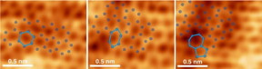 |
| Graphene, a super tough wonder material, hasn't made it into electronics yet because it doesn't conduct an electric current on its own. Researchers used a laser technique to permanently stress graphene into a structure that allows the flow of electric current. CREDIT Purdue University image/Gary Cheng |
Abstract:
ABSTRACT
Asymmetric 3D Elastic-Plastic Strain-Modulated Electron Energy Structure in Monolayer Graphene by Laser Shocking
Maithilee Motlag1, Prashant Kumar1, Kevin Y. Hu1, Shengyu Jin1, Ji Li1, Jiayi Shao1, Xuan Yi1, Yen-Hsiang Lin2, Jenna C. Walrath2, Lei Tong3, Xinyu Huang3, Rachel S. Goldman2, Lei Ye3, and Gary J. Cheng1
1Purdue University, West Lafayette, IN, USA
2University of Michigan, Ann Arbor, MI, USA
3Huazhong University of Science and Technology, Wuhan, China
doi: 10.1002/adma.201900597
Graphene has a great potential to replace silicon in prospective semiconductor industries due to its outstanding electronic and transport properties; nonetheless, its lack of energy bandgap is a substantial limitation for practical applications. To date, straining graphene to break its lattice symmetry is perhaps the most efficient approach toward realizing bandgap tunability in graphene. However, due to the weak lattice deformation induced by uniaxial or in?plane shear strain, most strained graphene studies have yielded bandgaps <1 eV. In this work, a modulated inhomogeneous local asymmetric elastic-plastic straining is reported that utilizes GPa?level laser shocking at a high strain rate (dε/dt) ? 106-107 s?1, with excellent formability, inducing tunable bandgaps in graphene of up to 2.1 eV, as determined by scanning tunneling spectroscopy. High?resolution imaging and Raman spectroscopy reveal strain?induced modifications to the atomic and electronic structure in graphene and first?principles simulations predict the measured bandgap openings. Laser shock modulation of semimetallic graphene to a semiconducting material with controllable bandgap has the potential to benefit the electronic and optoelectronic industries.
Laser technique could unlock use of tough material for next-generation electronics: Researchers make graphene tunable, opening up its band gap to a record 2.1 electronvolts
West Lafayette, IN | Posted on May 30th, 2019In 2004, researchers discovered a super thin material that is at least a 100 times stronger than steel and the best known conductor of heat and electricity.
This means that the material, graphene, could bring faster electronics than is possible today with silicon.
But to truly be useful, graphene would need to carry an electric current that switches on and off, like what silicon does in the form of billions of transistors on a computer chip. This switching creates strings of 0s and 1s that a computer uses for processing information.
Purdue University researchers, in collaboration with the University of Michigan and the Huazhong University of Science and Technology, show how a laser technique could permanently stress graphene into having a structure that allows the flow of electric current.
This structure is a so-called "band gap." Electrons need to jump across this gap in order to become conduction electrons, which makes them capable of carrying electric current. But graphene doesn't naturally have a band gap.
Purdue researchers created and widened the band gap in graphene to a record 2.1 electronvolts. To function as a semiconductor such as silicon, the band gap would need to be at least the previous record of 0.5 electronvolts.
"This is the first time that an effort has achieved such high band gaps without affecting graphene itself, such as through chemical doping. We have purely strained the material," said Gary Cheng, professor of industrial engineering at Purdue, whose lab has investigated various ways to make graphene more useful for commercial applications.
The presence of a band gap allows semiconductor materials to switch between insulating or conducting an electric current, depending on whether their electrons are pushed across the band gap or not.
Surpassing 0.5 electronvolts unlocks even more potential for graphene in next-generation electronic devices, the researchers say. Their work appears in an issue of Advanced Materials.
"Researchers in the past opened the band gap by simply stretching graphene, but stretching alone doesn't widen the band gap very much. You need to permanently change the shape of graphene to keep the band gap open," Cheng said.
Cheng and his collaborators not only kept the band gap open in graphene, but also made it to where the gap width could be tuned from zero to 2.1 electronvolts, giving scientists and manufacturers the option to just use certain properties of graphene depending on what they want the material to do.
The researchers made the band gap structure permanent in graphene using a technique called laser shock imprinting, which Cheng developed in 2014 along with scientists at Harvard University, the Madrid Institute for Advanced Studies and the University of California, San Diego.
For this study, the researchers used a laser to create shockwave impulses that penetrated an underlying sheet of graphene. The laser shock strains graphene onto a trench-like mold - permanently shaping it. Adjusting the laser power adjusts the band gap.
While still far from putting graphene into semiconducting devices, the technique grants more flexibility in taking advantage of the material's optical, magnetic and thermal properties, Cheng said.
###
The work was supported by multiple entities, including the National Science Foundation (Grant numbers CMMI-0547636 and CMMI 0928752) and the National Research Council Senior Research Associateship.
####
For more information, please click here
Contacts:
Kayla Wiles
765-494-2432
Copyright © Purdue University
If you have a comment, please Contact us.Issuers of news releases, not 7th Wave, Inc. or Nanotechnology Now, are solely responsible for the accuracy of the content.
Bookmark:


| Related Links |
| Related News Press |
News and information
![]() Quantum computer improves AI predictions April 17th, 2026
Quantum computer improves AI predictions April 17th, 2026
![]() Flexible sensor gains sensitivity under pressure April 17th, 2026
Flexible sensor gains sensitivity under pressure April 17th, 2026
![]() A reusable chip for particulate matter sensing April 17th, 2026
A reusable chip for particulate matter sensing April 17th, 2026
![]() Detecting vibrational quantum beating in the predissociation dynamics of SF6 using time-resolved photoelectron spectroscopy April 17th, 2026
Detecting vibrational quantum beating in the predissociation dynamics of SF6 using time-resolved photoelectron spectroscopy April 17th, 2026
2 Dimensional Materials
![]() Flexible sensor gains sensitivity under pressure April 17th, 2026
Flexible sensor gains sensitivity under pressure April 17th, 2026
![]() MXene nanomaterials enter a new dimension Multilayer nanomaterial: MXene flakes created at Drexel University show new promise as 1D scrolls January 30th, 2026
MXene nanomaterials enter a new dimension Multilayer nanomaterial: MXene flakes created at Drexel University show new promise as 1D scrolls January 30th, 2026
![]() ICFO researchers overcome long-standing bottleneck in single photon detection with twisted 2D materials August 8th, 2025
ICFO researchers overcome long-standing bottleneck in single photon detection with twisted 2D materials August 8th, 2025
Magnetism/Magnons
![]() Metasurfaces smooth light to boost magnetic sensing precision January 30th, 2026
Metasurfaces smooth light to boost magnetic sensing precision January 30th, 2026
![]() Researchers develop molecular qubits that communicate at telecom frequencies October 3rd, 2025
Researchers develop molecular qubits that communicate at telecom frequencies October 3rd, 2025
![]() Magnetism in new exotic material opens the way for robust quantum computers June 4th, 2025
Magnetism in new exotic material opens the way for robust quantum computers June 4th, 2025
Graphene/ Graphite
![]() Electrifying results shed light on graphene foam as a potential material for lab grown cartilage June 6th, 2025
Electrifying results shed light on graphene foam as a potential material for lab grown cartilage June 6th, 2025
Govt.-Legislation/Regulation/Funding/Policy
![]() Quantum computer improves AI predictions April 17th, 2026
Quantum computer improves AI predictions April 17th, 2026
![]() Metasurfaces smooth light to boost magnetic sensing precision January 30th, 2026
Metasurfaces smooth light to boost magnetic sensing precision January 30th, 2026
![]() New imaging approach transforms study of bacterial biofilms August 8th, 2025
New imaging approach transforms study of bacterial biofilms August 8th, 2025
Possible Futures
![]() A fundamentally new therapeutic approach to cystic fibrosis: Nanobody repairs cellular defect April 17th, 2026
A fundamentally new therapeutic approach to cystic fibrosis: Nanobody repairs cellular defect April 17th, 2026
![]() UC Irvine physicists discover method to reverse �quantum scrambling� : The work addresses the problem of information loss in quantum computing system April 17th, 2026
UC Irvine physicists discover method to reverse �quantum scrambling� : The work addresses the problem of information loss in quantum computing system April 17th, 2026
Chip Technology
![]() A reusable chip for particulate matter sensing April 17th, 2026
A reusable chip for particulate matter sensing April 17th, 2026
![]() Metasurfaces smooth light to boost magnetic sensing precision January 30th, 2026
Metasurfaces smooth light to boost magnetic sensing precision January 30th, 2026
Nanoelectronics
![]() Lab to industry: InSe wafer-scale breakthrough for future electronics August 8th, 2025
Lab to industry: InSe wafer-scale breakthrough for future electronics August 8th, 2025
![]() Interdisciplinary: Rice team tackles the future of semiconductors Multiferroics could be the key to ultralow-energy computing October 6th, 2023
Interdisciplinary: Rice team tackles the future of semiconductors Multiferroics could be the key to ultralow-energy computing October 6th, 2023
![]() Key element for a scalable quantum computer: Physicists from Forschungszentrum J�lich and RWTH Aachen University demonstrate electron transport on a quantum chip September 23rd, 2022
Key element for a scalable quantum computer: Physicists from Forschungszentrum J�lich and RWTH Aachen University demonstrate electron transport on a quantum chip September 23rd, 2022
![]() Reduced power consumption in semiconductor devices September 23rd, 2022
Reduced power consumption in semiconductor devices September 23rd, 2022
Discoveries
![]() Quantum computer improves AI predictions April 17th, 2026
Quantum computer improves AI predictions April 17th, 2026
![]() Flexible sensor gains sensitivity under pressure April 17th, 2026
Flexible sensor gains sensitivity under pressure April 17th, 2026
![]() A reusable chip for particulate matter sensing April 17th, 2026
A reusable chip for particulate matter sensing April 17th, 2026
![]() Detecting vibrational quantum beating in the predissociation dynamics of SF6 using time-resolved photoelectron spectroscopy April 17th, 2026
Detecting vibrational quantum beating in the predissociation dynamics of SF6 using time-resolved photoelectron spectroscopy April 17th, 2026
Materials/Metamaterials/Magnetoresistance
![]() First real-time observation of two-dimensional melting process: Researchers at Mainz University unveil new insights into magnetic vortex structures August 8th, 2025
First real-time observation of two-dimensional melting process: Researchers at Mainz University unveil new insights into magnetic vortex structures August 8th, 2025
![]() Researchers unveil a groundbreaking clay-based solution to capture carbon dioxide and combat climate change June 6th, 2025
Researchers unveil a groundbreaking clay-based solution to capture carbon dioxide and combat climate change June 6th, 2025
![]() A 1960s idea inspires NBI researchers to study hitherto inaccessible quantum states June 6th, 2025
A 1960s idea inspires NBI researchers to study hitherto inaccessible quantum states June 6th, 2025
![]() Institute for Nanoscience hosts annual proposal planning meeting May 16th, 2025
Institute for Nanoscience hosts annual proposal planning meeting May 16th, 2025
Announcements
![]() A fundamentally new therapeutic approach to cystic fibrosis: Nanobody repairs cellular defect April 17th, 2026
A fundamentally new therapeutic approach to cystic fibrosis: Nanobody repairs cellular defect April 17th, 2026
![]() UC Irvine physicists discover method to reverse �quantum scrambling� : The work addresses the problem of information loss in quantum computing system April 17th, 2026
UC Irvine physicists discover method to reverse �quantum scrambling� : The work addresses the problem of information loss in quantum computing system April 17th, 2026
Interviews/Book Reviews/Essays/Reports/Podcasts/Journals/White papers/Posters
![]() A fundamentally new therapeutic approach to cystic fibrosis: Nanobody repairs cellular defect April 17th, 2026
A fundamentally new therapeutic approach to cystic fibrosis: Nanobody repairs cellular defect April 17th, 2026
![]() UC Irvine physicists discover method to reverse �quantum scrambling� : The work addresses the problem of information loss in quantum computing system April 17th, 2026
UC Irvine physicists discover method to reverse �quantum scrambling� : The work addresses the problem of information loss in quantum computing system April 17th, 2026
Photonics/Optics/Lasers
![]() Metasurfaces smooth light to boost magnetic sensing precision January 30th, 2026
Metasurfaces smooth light to boost magnetic sensing precision January 30th, 2026
![]() From sensors to smart systems: the rise of AI-driven photonic noses January 30th, 2026
From sensors to smart systems: the rise of AI-driven photonic noses January 30th, 2026
Research partnerships
![]() Lab to industry: InSe wafer-scale breakthrough for future electronics August 8th, 2025
Lab to industry: InSe wafer-scale breakthrough for future electronics August 8th, 2025
![]() HKU physicists uncover hidden order in the quantum world through deconfined quantum critical points April 25th, 2025
HKU physicists uncover hidden order in the quantum world through deconfined quantum critical points April 25th, 2025
|
|
||
|
|
||
| The latest news from around the world, FREE | ||
|
|
||
|
|
||
| Premium Products | ||
|
|
||
|
Only the news you want to read!
Learn More |
||
|
|
||
|
Full-service, expert consulting
Learn More |
||
|
|
||