Home > Press > Squeezed nanocrystals: A new model predicts their shape when blanketed under graphene
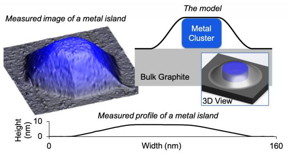 |
| Ames Laboratory and Northeastern University developed and validated a model that predicts the shape of metal nanoparticles blanketed by 2D material. The top blanket of graphene resists deformation, 'squeezing' downward on the metal nanoparticle and forcing it to be extremely low and wide. CREDIT US Department of Energy, Ames Laboratory |
Abstract:
In a collaboration between the U.S. Department of Energy's Ames Laboratory and Northeastern University, scientists have developed a model for predicting the shape of metal nanocrystals or "islands" sandwiched between or below two-dimensional (2D) materials such as graphene. The advance moves 2D quantum materials a step closer to applications in electronics.
Squeezed nanocrystals: A new model predicts their shape when blanketed under graphene
Ames, IA | Posted on April 5th, 2019Ames Laboratory scientist are experts in 2D materials, and recently discovered a first-of-its-kind copper and graphite combination, produced by depositing copper on ion-bombarded graphite at high temperature and in an ultra-high vacuum environment. This produced a distribution of copper islands, embedded under an ultra-thin "blanket" consisting of a few layers of graphene.
"Because these metal islands can potentially serve as electrical contacts or heat sinks in electronic applications, their shape and how they reach that shape are important pieces of information in controlling the design and synthesis of these materials," said Pat Thiel, an Ames Laboratory scientist and Distinguished Professor of Chemistry and Materials Science and Engineering at Iowa State University.
Ames Laboratory scientists used scanning tunneling microscopy to painstakingly measure the shapes of more than a hundred nanometer-scale copper islands. This provided the experimental basis for a theoretical model developed jointly by researchers at Northeastern University's Department of Mechanical and Industrial Engineering and at Ames Laboratory. The model served to explain the data extremely well. The one exception, concerning copper islands less than 10 nm tall, will be the basis for further research.
"We love to see our physics applied, and this was a beautiful way to apply it," said Scott E. Julien, Ph.D. candidate, at Northeastern. "We were able to model the elastic response of the graphene as it drapes over the copper islands, and use it to predict the shapes of the islands."
The work showed that the top layer of graphene resists the upward pressure exerted by the growing metal island. In effect, the graphene layer squeezes downward and flattens the copper islands. Accounting for these effects as well as other key energetics leads to the unanticipated prediction of a universal, or size-independent, shape of the islands, at least for sufficiently-large islands of a given metal.
"This principle should work with other metals and other layered materials as well," said Research Assistant, Ann Lii-Rosales. "Experimentally we want to see if we can use the same recipe to synthesize metals under other types of layered materials with predictable results."
###
The research is further discussed in the paper, "Squeezed Nanocrystals: Equilibrium Configuration of Metal Clusters Embedded Beneath the Surface of a Layered Material," authored by Scott E. Julien, Ann Lii-Rosales, Kai-Tak Wan, Yong Han, Michael C. Tringides, James W. Evans, and Patricia A. Thiel; and published in Nanoscale.
The research was a collaboration between Ames Laboratory and Northeastern University.
Work at Northeastern University was supported by the National Institute of Standards and Technology (NIST), a national facility operated under the U.S. Department of Commerce.
Work at Ames Laboratory was supported primarily by the U.S. Department of Energy Office of Science. This work was also supported in part by a grant of computer time at the National Energy Research Scientific Computing Centre (NERSC), a DOE Office of Science User Facility.
####
About Ames Laboratory
Ames Laboratory is a U.S. Department of Energy Office of Science national laboratory operated by Iowa State University. Ames Laboratory creates innovative materials, technologies and energy solutions. We use our expertise, unique capabilities and interdisciplinary collaborations to solve global problems.
DOE's Office of Science is the single largest supporter of basic research in the physical sciences in the United States, and is working to address some of the most pressing challenges of our time. For more information, please visit science.energy.gov.
For more information, please click here
Contacts:
Laura Millsaps
Copyright © Ames Laboratory
If you have a comment, please Contact us.Issuers of news releases, not 7th Wave, Inc. or Nanotechnology Now, are solely responsible for the accuracy of the content.
Bookmark:


| Related News Press |
News and information
![]() Quantum computer improves AI predictions April 17th, 2026
Quantum computer improves AI predictions April 17th, 2026
![]() Flexible sensor gains sensitivity under pressure April 17th, 2026
Flexible sensor gains sensitivity under pressure April 17th, 2026
![]() A reusable chip for particulate matter sensing April 17th, 2026
A reusable chip for particulate matter sensing April 17th, 2026
![]() Detecting vibrational quantum beating in the predissociation dynamics of SF6 using time-resolved photoelectron spectroscopy April 17th, 2026
Detecting vibrational quantum beating in the predissociation dynamics of SF6 using time-resolved photoelectron spectroscopy April 17th, 2026
2 Dimensional Materials
![]() Flexible sensor gains sensitivity under pressure April 17th, 2026
Flexible sensor gains sensitivity under pressure April 17th, 2026
![]() ICFO researchers overcome long-standing bottleneck in single photon detection with twisted 2D materials August 8th, 2025
ICFO researchers overcome long-standing bottleneck in single photon detection with twisted 2D materials August 8th, 2025
![]() First real-time observation of two-dimensional melting process: Researchers at Mainz University unveil new insights into magnetic vortex structures August 8th, 2025
First real-time observation of two-dimensional melting process: Researchers at Mainz University unveil new insights into magnetic vortex structures August 8th, 2025
![]() Lab to industry: InSe wafer-scale breakthrough for future electronics August 8th, 2025
Lab to industry: InSe wafer-scale breakthrough for future electronics August 8th, 2025
Laboratories
![]() Researchers develop molecular qubits that communicate at telecom frequencies October 3rd, 2025
Researchers develop molecular qubits that communicate at telecom frequencies October 3rd, 2025
Graphene/ Graphite
![]() Electrifying results shed light on graphene foam as a potential material for lab grown cartilage June 6th, 2025
Electrifying results shed light on graphene foam as a potential material for lab grown cartilage June 6th, 2025
![]() Breakthrough in proton barrier films using pore-free graphene oxide: Kumamoto University researchers achieve new milestone in advanced coating technologies September 13th, 2024
Breakthrough in proton barrier films using pore-free graphene oxide: Kumamoto University researchers achieve new milestone in advanced coating technologies September 13th, 2024
Govt.-Legislation/Regulation/Funding/Policy
![]() Quantum computer improves AI predictions April 17th, 2026
Quantum computer improves AI predictions April 17th, 2026
![]() Metasurfaces smooth light to boost magnetic sensing precision January 30th, 2026
Metasurfaces smooth light to boost magnetic sensing precision January 30th, 2026
![]() New imaging approach transforms study of bacterial biofilms August 8th, 2025
New imaging approach transforms study of bacterial biofilms August 8th, 2025
Possible Futures
![]() A fundamentally new therapeutic approach to cystic fibrosis: Nanobody repairs cellular defect April 17th, 2026
A fundamentally new therapeutic approach to cystic fibrosis: Nanobody repairs cellular defect April 17th, 2026
![]() UC Irvine physicists discover method to reverse �quantum scrambling� : The work addresses the problem of information loss in quantum computing system April 17th, 2026
UC Irvine physicists discover method to reverse �quantum scrambling� : The work addresses the problem of information loss in quantum computing system April 17th, 2026
Chip Technology
![]() A reusable chip for particulate matter sensing April 17th, 2026
A reusable chip for particulate matter sensing April 17th, 2026
![]() Metasurfaces smooth light to boost magnetic sensing precision January 30th, 2026
Metasurfaces smooth light to boost magnetic sensing precision January 30th, 2026
Discoveries
![]() Quantum computer improves AI predictions April 17th, 2026
Quantum computer improves AI predictions April 17th, 2026
![]() Flexible sensor gains sensitivity under pressure April 17th, 2026
Flexible sensor gains sensitivity under pressure April 17th, 2026
![]() A reusable chip for particulate matter sensing April 17th, 2026
A reusable chip for particulate matter sensing April 17th, 2026
![]() Detecting vibrational quantum beating in the predissociation dynamics of SF6 using time-resolved photoelectron spectroscopy April 17th, 2026
Detecting vibrational quantum beating in the predissociation dynamics of SF6 using time-resolved photoelectron spectroscopy April 17th, 2026
Materials/Metamaterials/Magnetoresistance
![]() First real-time observation of two-dimensional melting process: Researchers at Mainz University unveil new insights into magnetic vortex structures August 8th, 2025
First real-time observation of two-dimensional melting process: Researchers at Mainz University unveil new insights into magnetic vortex structures August 8th, 2025
![]() Researchers unveil a groundbreaking clay-based solution to capture carbon dioxide and combat climate change June 6th, 2025
Researchers unveil a groundbreaking clay-based solution to capture carbon dioxide and combat climate change June 6th, 2025
![]() A 1960s idea inspires NBI researchers to study hitherto inaccessible quantum states June 6th, 2025
A 1960s idea inspires NBI researchers to study hitherto inaccessible quantum states June 6th, 2025
![]() Institute for Nanoscience hosts annual proposal planning meeting May 16th, 2025
Institute for Nanoscience hosts annual proposal planning meeting May 16th, 2025
Announcements
![]() A fundamentally new therapeutic approach to cystic fibrosis: Nanobody repairs cellular defect April 17th, 2026
A fundamentally new therapeutic approach to cystic fibrosis: Nanobody repairs cellular defect April 17th, 2026
![]() UC Irvine physicists discover method to reverse �quantum scrambling� : The work addresses the problem of information loss in quantum computing system April 17th, 2026
UC Irvine physicists discover method to reverse �quantum scrambling� : The work addresses the problem of information loss in quantum computing system April 17th, 2026
Research partnerships
![]() Lab to industry: InSe wafer-scale breakthrough for future electronics August 8th, 2025
Lab to industry: InSe wafer-scale breakthrough for future electronics August 8th, 2025
![]() HKU physicists uncover hidden order in the quantum world through deconfined quantum critical points April 25th, 2025
HKU physicists uncover hidden order in the quantum world through deconfined quantum critical points April 25th, 2025
|
|
||
|
|
||
| The latest news from around the world, FREE | ||
|
|
||
|
|
||
| Premium Products | ||
|
|
||
|
Only the news you want to read!
Learn More |
||
|
|
||
|
Full-service, expert consulting
Learn More |
||
|
|
||