Home > Press > Device makes power conversion more efficient: New design could dramatically cut energy waste in electric vehicles, data centers, and the power grid
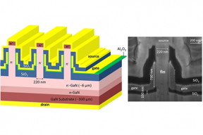 |
| “Instead of doing the complicated zigzag path for the current in conventional vertical transistors,” Professor Tomás Palacios says, “let’s change the geometry of the transistor completely.” Their vertical gallium nitride transistors have bladelike protrusions on top, known as “fins.” The narrowness of the fin ensures that the gate electrode will be able to switch the transistor on and off. Courtesy of the researchers |
Abstract:
Power electronics, which do things like modify voltages or convert between direct and alternating current, are everywhere. They’re in the power bricks we use to charge our portable devices; they’re in the battery packs of electric cars; and they’re in the power grid itself, where they mediate between high-voltage transmission lines and the lower voltages of household electrical sockets.
Device makes power conversion more efficient: New design could dramatically cut energy waste in electric vehicles, data centers, and the power grid
Cambridge, MA | Posted on December 8th, 2017ower conversion is intrinsically inefficient: A power converter will never output quite as much power as it takes in. But recently, power converters made from gallium nitride have begun to reach the market, boasting higher efficiencies and smaller sizes than conventional, silicon-based power converters.
Commercial gallium nitride power devices can’t handle voltages above about 600 volts, however, which limits their use to household electronics.
At the Institute of Electrical and Electronics Engineers’ International Electron Devices Meeting this week, researchers from MIT, semiconductor company IQE, Columbia University, IBM, and the Singapore-MIT Alliance for Research and Technology, presented a new design that, in tests, enabled gallium nitride power devices to handle voltages of 1,200 volts.
That’s already enough capacity for use in electric vehicles, but the researchers emphasize that their device is a first prototype manufactured in an academic lab. They believe that further work can boost its capacity to the 3,300-to-5,000-volt range, to bring the efficiencies of gallium nitride to the power electronics in the electrical grid itself.
That’s because the new device uses a fundamentally different design from existing gallium nitride power electronics.
“All the devices that are commercially available are what are called lateral devices,” says Tomás Palacios, who is an MIT professor of electrical engineering and computer science, a member of the Microsystems Technology Laboratories, and senior author on the new paper. “So the entire device is fabricated on the top surface of the gallium nitride wafer, which is good for low-power applications like the laptop charger. But for medium- and high-power applications, vertical devices are much better. These are devices where the current, instead of flowing through the surface of the semiconductor, flows through the wafer, across the semiconductor. Vertical devices are much better in terms of how much voltage they can manage and how much current they control.”
For one thing, Palacios explains, current flows into one surface of a vertical device and out the other. That means that there’s simply more space in which to attach input and output wires, which enables higher current loads.
For another, Palacios says, “when you have lateral devices, all the current flows through a very narrow slab of material close to the surface. We are talking about a slab of material that could be just 50 nanometers in thickness. So all the current goes through there, and all the heat is being generated in that very narrow region, so it gets really, really, really hot. In a vertical device, the current flows through the entire wafer, so the heat dissipation is much more uniform.”
Narrowing the field
Although their advantages are well-known, vertical devices have been difficult to fabricate in gallium nitride. Power electronics depend on transistors, devices in which a charge applied to a “gate” switches a semiconductor material — such as silicon or gallium nitride — between a conductive and a nonconductive state.
For that switching to be efficient, the current flowing through the semiconductor needs to be confined to a relatively small area, where the gate’s electric field can exert an influence on it. In the past, researchers had attempted to build vertical transistors by embedding physical barriers in the gallium nitride to direct current into a channel beneath the gate.
But the barriers are built from a temperamental material that’s costly and difficult to produce, and integrating it with the surrounding gallium nitride in a way that doesn’t disrupt the transistor’s electronic properties has also proven challenging.
Palacios and his collaborators adopt a simple but effective alternative. The team includes first authors Yuhao Zhang, a postdoc in Palacios’s lab, and Min Sun, who received his MIT PhD in the Department of Electrical Engineering and Computer Science (EECS) last spring; Daniel Piedra and Yuxuan Lin, MIT graduate students in EECS; Jie Hu, a postdoc in Palacios’s group; Zhihong Liu of the Singapore-MIT Alliance for Research and Technology; Xiang Gao of IQE; and Columbia’s Ken Shepard.
Rather than using an internal barrier to route current into a narrow region of a larger device, they simply use a narrower device. Their vertical gallium nitride transistors have bladelike protrusions on top, known as “fins.” On both sides of each fin are electrical contacts that together act as a gate. Current enters the transistor through another contact, on top of the fin, and exits through the bottom of the device. The narrowness of the fin ensures that the gate electrode will be able to switch the transistor on and off.
“Yuhao and Min’s brilliant idea, I think, was to say, ‘Instead of confining the current by having multiple materials in the same wafer, let’s confine it geometrically by removing the material from those regions where we don’t want the current to flow,’” Palacios says. “Instead of doing the complicated zigzag path for the current in conventional vertical transistors, let’s change the geometry of the transistor completely.”
###
Written by Larry Hardesty, MIT News Office
####
For more information, please click here
Contacts:
Abby Abazorius
MIT News Office
617.253.2709
Copyright © Massachusetts Institute of Technology
If you have a comment, please Contact us.Issuers of news releases, not 7th Wave, Inc. or Nanotechnology Now, are solely responsible for the accuracy of the content.
Bookmark:


| Related News Press |
News and information
![]() Quantum computer improves AI predictions April 17th, 2026
Quantum computer improves AI predictions April 17th, 2026
![]() Flexible sensor gains sensitivity under pressure April 17th, 2026
Flexible sensor gains sensitivity under pressure April 17th, 2026
![]() A reusable chip for particulate matter sensing April 17th, 2026
A reusable chip for particulate matter sensing April 17th, 2026
![]() Detecting vibrational quantum beating in the predissociation dynamics of SF6 using time-resolved photoelectron spectroscopy April 17th, 2026
Detecting vibrational quantum beating in the predissociation dynamics of SF6 using time-resolved photoelectron spectroscopy April 17th, 2026
Possible Futures
![]() A fundamentally new therapeutic approach to cystic fibrosis: Nanobody repairs cellular defect April 17th, 2026
A fundamentally new therapeutic approach to cystic fibrosis: Nanobody repairs cellular defect April 17th, 2026
![]() UC Irvine physicists discover method to reverse ‘quantum scrambling’ : The work addresses the problem of information loss in quantum computing system April 17th, 2026
UC Irvine physicists discover method to reverse ‘quantum scrambling’ : The work addresses the problem of information loss in quantum computing system April 17th, 2026
Chip Technology
![]() A reusable chip for particulate matter sensing April 17th, 2026
A reusable chip for particulate matter sensing April 17th, 2026
![]() Metasurfaces smooth light to boost magnetic sensing precision January 30th, 2026
Metasurfaces smooth light to boost magnetic sensing precision January 30th, 2026
Discoveries
![]() Quantum computer improves AI predictions April 17th, 2026
Quantum computer improves AI predictions April 17th, 2026
![]() Flexible sensor gains sensitivity under pressure April 17th, 2026
Flexible sensor gains sensitivity under pressure April 17th, 2026
![]() A reusable chip for particulate matter sensing April 17th, 2026
A reusable chip for particulate matter sensing April 17th, 2026
![]() Detecting vibrational quantum beating in the predissociation dynamics of SF6 using time-resolved photoelectron spectroscopy April 17th, 2026
Detecting vibrational quantum beating in the predissociation dynamics of SF6 using time-resolved photoelectron spectroscopy April 17th, 2026
Announcements
![]() A fundamentally new therapeutic approach to cystic fibrosis: Nanobody repairs cellular defect April 17th, 2026
A fundamentally new therapeutic approach to cystic fibrosis: Nanobody repairs cellular defect April 17th, 2026
![]() UC Irvine physicists discover method to reverse ‘quantum scrambling’ : The work addresses the problem of information loss in quantum computing system April 17th, 2026
UC Irvine physicists discover method to reverse ‘quantum scrambling’ : The work addresses the problem of information loss in quantum computing system April 17th, 2026
Interviews/Book Reviews/Essays/Reports/Podcasts/Journals/White papers/Posters
![]() A fundamentally new therapeutic approach to cystic fibrosis: Nanobody repairs cellular defect April 17th, 2026
A fundamentally new therapeutic approach to cystic fibrosis: Nanobody repairs cellular defect April 17th, 2026
![]() UC Irvine physicists discover method to reverse ‘quantum scrambling’ : The work addresses the problem of information loss in quantum computing system April 17th, 2026
UC Irvine physicists discover method to reverse ‘quantum scrambling’ : The work addresses the problem of information loss in quantum computing system April 17th, 2026
Automotive/Transportation
![]() Decoding hydrogen‑bond network of electrolyte for cryogenic durable aqueous zinc‑ion batteries January 30th, 2026
Decoding hydrogen‑bond network of electrolyte for cryogenic durable aqueous zinc‑ion batteries January 30th, 2026
![]() Sensors innovations for smart lithium-based batteries: advancements, opportunities, and potential challenges August 8th, 2025
Sensors innovations for smart lithium-based batteries: advancements, opportunities, and potential challenges August 8th, 2025
![]() Simple algorithm paired with standard imaging tool could predict failure in lithium metal batteries August 8th, 2025
Simple algorithm paired with standard imaging tool could predict failure in lithium metal batteries August 8th, 2025
Battery Technology/Capacitors/Generators/Piezoelectrics/Thermoelectrics/Energy storage
![]() Decoding hydrogen‑bond network of electrolyte for cryogenic durable aqueous zinc‑ion batteries January 30th, 2026
Decoding hydrogen‑bond network of electrolyte for cryogenic durable aqueous zinc‑ion batteries January 30th, 2026
![]() COF scaffold membrane with gate‑lane nanostructure for efficient Li+/Mg2+ separation January 30th, 2026
COF scaffold membrane with gate‑lane nanostructure for efficient Li+/Mg2+ separation January 30th, 2026
![]() MXene nanomaterials enter a new dimension Multilayer nanomaterial: MXene flakes created at Drexel University show new promise as 1D scrolls January 30th, 2026
MXene nanomaterials enter a new dimension Multilayer nanomaterial: MXene flakes created at Drexel University show new promise as 1D scrolls January 30th, 2026
|
|
||
|
|
||
| The latest news from around the world, FREE | ||
|
|
||
|
|
||
| Premium Products | ||
|
|
||
|
Only the news you want to read!
Learn More |
||
|
|
||
|
Full-service, expert consulting
Learn More |
||
|
|
||