Home > Press > Metal-silicone microstructures could enable new flexible optical and electrical devices: Laser-based method creates force-sensitive, flexible microstructures that conduct electricity
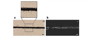 |
| Using a one-step laser fabrication process, researchers created flexible hybrid microwires that conduct electricity. (a) An optical microscope image of the silver (black) and silicone (clear) microwires. (b) Scanning electron microscopy image of the same fabricated structure. Both scale bars are equal to 25 microns. CREDIT Mitsuhiro Terakawa, Keio University |
Abstract:
For the first time, researchers have used a single-step, laser-based method to produce small, precise hybrid microstructures of silver and flexible silicone. This innovative laser processing technology could one day enable smart factories that use one production line to mass-produce customized devices combining soft materials such as engineered tissue with hard materials that add functions such as glucose sensing.
Metal-silicone microstructures could enable new flexible optical and electrical devices: Laser-based method creates force-sensitive, flexible microstructures that conduct electricity
Washington, DC | Posted on November 1st, 2017The metal component of the microstructures renders them electrically conductive while the elastic silicone contributes flexibility. This unique combination of properties makes the structures sensitive to mechanical force and could be useful for making new types of optical and electrical devices.
"These types of microstructures could possibly be used to measure very small movements or changes, such as a slight movement from an insect's body or the subtle expression produced by a human facial muscle," said research team leader Mitsuhiro Terakawa from Keio University, Japan. "This information could be used to create perfect computer-generated versions of these movements."
As detailed in the journal Optical Materials Express, from The Optical Society (OSA), the researchers produced wire-like structures of silver surrounded by a type of silicone known as polydimethylsiloxane (PDMS). The researchers used PDMS because it is flexible and biocompatible, meaning that it is safer to use on or in the body.
They fabricated the structures, which measure as little as 25 microns wide, by irradiating a mixture of PDMS and silver ions with extremely short laser pulses that last just femtoseconds. In one femtosecond, light travels only 300 nanometers, which is just slightly larger than the smallest bacteria.
"We believe we are the first group to use femtosecond laser pulses to create a hybrid material containing PDMS, which is very useful because of its elasticity," said Terakawa. "The work represents a step towards using a single, precision laser processing technology to fabricate biocompatible devices that combine hard and soft materials."
Turning two laser processes into one
The one-step fabrication method used to make the hybrid microstructures combines the light-based chemical reactions known as photopolymerization and photoreduction, both of which were induced using femtosecond laser pulses. Photopolymerization uses light to harden a polymer, and photoreduction uses light to form microstructures and nanostructures from metal ions.
The fabrication technique resulted from a collaboration between Terakawa's research group, which been studying two-photon photoreduction using soft materials, and a group at the German research organization Laser Zentrum Hannover, that has been advancing single-photon photopolymerization of PDMS.
To create the wire microstructures, the researchers irradiated the PDMS-silver mixture with light from femtosecond laser emitting at 522-nm, a wavelength that interacts efficiently with the material mixture. They also carefully selected silver ions that would combine well with PDMS.
The researchers found that just one laser scan formed wires that exhibit both the electrical conductivity of metal and the elasticity of a polymer. Additional scans could be used to produce thicker and more uniform structures. They also showed that the wire structures responded to mechanical force by blowing air over the structures to create a pressure of 3 kilopascal.
The researchers say that, in addition to making wires structures, the approach could be used to make tiny 3D metal-silicone structures. As a next step, they plan to study whether the fabricated wires maintain their structure and properties over time.
"Our work demonstrates that simultaneously inducing photoreduction and photopolymerization is a promising method for fabricating elastic and electrically conductive microstructures," said Terakawa. "This is one step toward our long-term goal of developing a smart factory for fabricating many human-compatible devices in one production line, whether the materials are soft or hard."
####
About The Optical Society
Founded in 1916, The Optical Society (OSA) is the leading professional organization for scientists, engineers, students and business leaders who fuel discoveries, shape real-life applications and accelerate achievements in the science of light. Through world-renowned publications, meetings and membership initiatives, OSA provides quality research, inspired interactions and dedicated resources for its extensive global network of optics and photonics experts. For more information, visit osa.org.
About Optical Materials Express
Optical Materials Express (OMEx) is an open-access journal focusing on the synthesis, processing and characterization of materials for applications in optics and photonics. OMEx, which launched in April 2011, primarily emphasizes advances in novel optical materials, their properties, modeling, synthesis and fabrication techniques; how such materials contribute to novel optical behavior; and how they enable new or improved optical devices. The editor-in-chief for OMEx is Alexandra Boltasseva from Purdue University. For more information, visit: OSA Publishing.
For more information, please click here
Contacts:
Joshua Miller
202-416-1435
Rebecca B. Andersen
The Optical Society
1 202.416.1443
Copyright © The Optical Society
If you have a comment, please Contact us.Issuers of news releases, not 7th Wave, Inc. or Nanotechnology Now, are solely responsible for the accuracy of the content.
Bookmark:


| Related Links |
| Related News Press |
News and information
![]() Quantum computer improves AI predictions April 17th, 2026
Quantum computer improves AI predictions April 17th, 2026
![]() Flexible sensor gains sensitivity under pressure April 17th, 2026
Flexible sensor gains sensitivity under pressure April 17th, 2026
![]() A reusable chip for particulate matter sensing April 17th, 2026
A reusable chip for particulate matter sensing April 17th, 2026
![]() Detecting vibrational quantum beating in the predissociation dynamics of SF6 using time-resolved photoelectron spectroscopy April 17th, 2026
Detecting vibrational quantum beating in the predissociation dynamics of SF6 using time-resolved photoelectron spectroscopy April 17th, 2026
Flexible Electronics
![]() Flexible sensor gains sensitivity under pressure April 17th, 2026
Flexible sensor gains sensitivity under pressure April 17th, 2026
Hardware
![]() The present and future of computing get a boost from new research July 21st, 2023
The present and future of computing get a boost from new research July 21st, 2023
![]() A Carbon Nanotube Microprocessor Mature Enough to Say Hello: Three new breakthroughs make commercial nanotube processors possible March 2nd, 2020
A Carbon Nanotube Microprocessor Mature Enough to Say Hello: Three new breakthroughs make commercial nanotube processors possible March 2nd, 2020
![]() Powering the future: Smallest all-digital circuit opens doors to 5 nm next-gen semiconductor February 11th, 2020
Powering the future: Smallest all-digital circuit opens doors to 5 nm next-gen semiconductor February 11th, 2020
Possible Futures
![]() A fundamentally new therapeutic approach to cystic fibrosis: Nanobody repairs cellular defect April 17th, 2026
A fundamentally new therapeutic approach to cystic fibrosis: Nanobody repairs cellular defect April 17th, 2026
![]() UC Irvine physicists discover method to reverse �quantum scrambling� : The work addresses the problem of information loss in quantum computing system April 17th, 2026
UC Irvine physicists discover method to reverse �quantum scrambling� : The work addresses the problem of information loss in quantum computing system April 17th, 2026
Optical computing/Photonic computing
![]() ICFO researchers overcome long-standing bottleneck in single photon detection with twisted 2D materials August 8th, 2025
ICFO researchers overcome long-standing bottleneck in single photon detection with twisted 2D materials August 8th, 2025
![]() Programmable electron-induced color router array May 14th, 2025
Programmable electron-induced color router array May 14th, 2025
Discoveries
![]() Quantum computer improves AI predictions April 17th, 2026
Quantum computer improves AI predictions April 17th, 2026
![]() Flexible sensor gains sensitivity under pressure April 17th, 2026
Flexible sensor gains sensitivity under pressure April 17th, 2026
![]() A reusable chip for particulate matter sensing April 17th, 2026
A reusable chip for particulate matter sensing April 17th, 2026
![]() Detecting vibrational quantum beating in the predissociation dynamics of SF6 using time-resolved photoelectron spectroscopy April 17th, 2026
Detecting vibrational quantum beating in the predissociation dynamics of SF6 using time-resolved photoelectron spectroscopy April 17th, 2026
Materials/Metamaterials/Magnetoresistance
![]() First real-time observation of two-dimensional melting process: Researchers at Mainz University unveil new insights into magnetic vortex structures August 8th, 2025
First real-time observation of two-dimensional melting process: Researchers at Mainz University unveil new insights into magnetic vortex structures August 8th, 2025
![]() Researchers unveil a groundbreaking clay-based solution to capture carbon dioxide and combat climate change June 6th, 2025
Researchers unveil a groundbreaking clay-based solution to capture carbon dioxide and combat climate change June 6th, 2025
![]() A 1960s idea inspires NBI researchers to study hitherto inaccessible quantum states June 6th, 2025
A 1960s idea inspires NBI researchers to study hitherto inaccessible quantum states June 6th, 2025
![]() Institute for Nanoscience hosts annual proposal planning meeting May 16th, 2025
Institute for Nanoscience hosts annual proposal planning meeting May 16th, 2025
Announcements
![]() A fundamentally new therapeutic approach to cystic fibrosis: Nanobody repairs cellular defect April 17th, 2026
A fundamentally new therapeutic approach to cystic fibrosis: Nanobody repairs cellular defect April 17th, 2026
![]() UC Irvine physicists discover method to reverse �quantum scrambling� : The work addresses the problem of information loss in quantum computing system April 17th, 2026
UC Irvine physicists discover method to reverse �quantum scrambling� : The work addresses the problem of information loss in quantum computing system April 17th, 2026
Interviews/Book Reviews/Essays/Reports/Podcasts/Journals/White papers/Posters
![]() A fundamentally new therapeutic approach to cystic fibrosis: Nanobody repairs cellular defect April 17th, 2026
A fundamentally new therapeutic approach to cystic fibrosis: Nanobody repairs cellular defect April 17th, 2026
![]() UC Irvine physicists discover method to reverse �quantum scrambling� : The work addresses the problem of information loss in quantum computing system April 17th, 2026
UC Irvine physicists discover method to reverse �quantum scrambling� : The work addresses the problem of information loss in quantum computing system April 17th, 2026
Photonics/Optics/Lasers
![]() Metasurfaces smooth light to boost magnetic sensing precision January 30th, 2026
Metasurfaces smooth light to boost magnetic sensing precision January 30th, 2026
![]() From sensors to smart systems: the rise of AI-driven photonic noses January 30th, 2026
From sensors to smart systems: the rise of AI-driven photonic noses January 30th, 2026
|
|
||
|
|
||
| The latest news from around the world, FREE | ||
|
|
||
|
|
||
| Premium Products | ||
|
|
||
|
Only the news you want to read!
Learn More |
||
|
|
||
|
Full-service, expert consulting
Learn More |
||
|
|
||