Home > Press > UnitySC Announces Wafer Thinning Inspection System; Win from Power Semiconductor IDM for Automotive: Leading IDM Selects New 4See Series Automated Defect Inspection Platform for Power Semiconductor Automotive Applications
 |
Abstract:
UnitySC, a leader in advanced inspection and metrology solutions, today announced multiple orders from a leading integrated device manufacturer (IDM) for its modular 4See Series automated defect inspection platform. The systems were selected because they deliver optimal wafer backside surface and edge defect inspection, post thinning and metallization. The 4See Series will be used for automotive applications by a market leader in power semiconductor manufacturing to improve the reliability and performance of its products.
UnitySC Announces Wafer Thinning Inspection System; Win from Power Semiconductor IDM for Automotive: Leading IDM Selects New 4See Series Automated Defect Inspection Platform for Power Semiconductor Automotive Applications
Grenoble, France | Posted on May 11th, 2017"Being selected by a market leader validates the strength of our solutions and confirms our strategy to address new markets with our advanced process control solutions," said Gilles Fresquet, CEO, UnitySC. "This win expands our reach beyond the traditional substrate control market to include wafer thinning for power semiconductors."
IHS Markit predicts USD $3 billion in global market growth for the power semiconductors used in cars and light passenger vehicles, over the next six years. Increasing electronic content is a key driver, particularly in hybrid and electric cars, due to consumer demand for constant connectivity. The automotive industry�s push to deliver autonomous, green vehicles in the next decade is also driving growth. These technologies rely on the latest power semiconductor devices, enabled by advanced wafer manufacturing processes like wafer thinning.
�As the wafers used in power semiconductor manufacturing become thinner, controlling wafer quality through the backside thinning and metallization process steps becomes more critical to end-device performance and reliability,� noted Fresquet. �For years, manufacturers have considered our Deflector module to be the best-in-class solution for silicon and silicon-on-insulator wafer slip line detection. Combined with the Edge module, this 4See Series configuration delivers industry-leading inspection capabilities that meet semiconductor market needs.�
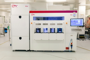
UnitySC�s new 4See Series for all-surface inspection of semiconductor wafers is a modular system with up to three module offerings: Deflector, Edge and LineScan. The platform can be configured according to application needs, such as wafer thinning, �bumping, MEMS, and more, and can include any number of the modules in desired configurations.
� Based on phase shift deflectometry technology, the Deflector module is a wafer surface inspection solution that achieves high throughput and very high vertical sensitivity in the nanometer range. It can detect slip lines, grinding marks, failures, cracks, comets, embedded particles, residue, and stains. The Deflector module is well suited to frontside and backside inspection, even under highly warped conditions.
� The Edge module is a high throughput and versatile solution based on confocal chromatic technology, which is used to inspect the full wafer edge: top, top bevel, apex, bottom bevel and bottom. It has a high depth of focus and does not require a backside contact chuck.
Combining the Deflector and Edge modules in one system offers full wafer characterization compliant with 8� or 12�� wafer high-volume manufacturing requirements. The 4See Series is scheduled to ship in Q3 2017 to fab locations around the world.
####
About UnitySC
UnitySC is recognized worldwide as a key player in inspection and metrology, combining advanced technologies in automated optical inspection and 3D imaging with microscopy, temporal-mode interferometry, and spectrometry, which enables customers to achieve higher yields and faster time to market. Customers include the largest foundries, integrated device manufacturers, outsourced semiconductor assembly and test service providers, and R&D centers. We provide standard and customized solutions adapted to specific industrial needs and constraints, enabling a new era in process control. Headquartered in Grenoble, France, the company maintains offices in Taiwan and is supported by a network of representatives and distributors.
For more information, please click here
Contacts:
Press Contact
Eric Lawson
Impress Labs
Tel: +1 480-276-9572
Copyright © UnitySC
If you have a comment, please Contact us.Issuers of news releases, not 7th Wave, Inc. or Nanotechnology Now, are solely responsible for the accuracy of the content.
Bookmark:


| Related News Press |
News and information
![]() Quantum computer improves AI predictions April 17th, 2026
Quantum computer improves AI predictions April 17th, 2026
![]() Flexible sensor gains sensitivity under pressure April 17th, 2026
Flexible sensor gains sensitivity under pressure April 17th, 2026
![]() A reusable chip for particulate matter sensing April 17th, 2026
A reusable chip for particulate matter sensing April 17th, 2026
![]() Detecting vibrational quantum beating in the predissociation dynamics of SF6 using time-resolved photoelectron spectroscopy April 17th, 2026
Detecting vibrational quantum beating in the predissociation dynamics of SF6 using time-resolved photoelectron spectroscopy April 17th, 2026
Imaging
![]() Simple algorithm paired with standard imaging tool could predict failure in lithium metal batteries August 8th, 2025
Simple algorithm paired with standard imaging tool could predict failure in lithium metal batteries August 8th, 2025
Announcements
![]() A fundamentally new therapeutic approach to cystic fibrosis: Nanobody repairs cellular defect April 17th, 2026
A fundamentally new therapeutic approach to cystic fibrosis: Nanobody repairs cellular defect April 17th, 2026
![]() UC Irvine physicists discover method to reverse �quantum scrambling� : The work addresses the problem of information loss in quantum computing system April 17th, 2026
UC Irvine physicists discover method to reverse �quantum scrambling� : The work addresses the problem of information loss in quantum computing system April 17th, 2026
Tools
![]() Metasurfaces smooth light to boost magnetic sensing precision January 30th, 2026
Metasurfaces smooth light to boost magnetic sensing precision January 30th, 2026
![]() From sensors to smart systems: the rise of AI-driven photonic noses January 30th, 2026
From sensors to smart systems: the rise of AI-driven photonic noses January 30th, 2026
![]() Japan launches fully domestically produced quantum computer: Expo visitors to experience quantum computing firsthand August 8th, 2025
Japan launches fully domestically produced quantum computer: Expo visitors to experience quantum computing firsthand August 8th, 2025
Automotive/Transportation
![]() Decoding hydrogen‑bond network of electrolyte for cryogenic durable aqueous zinc‑ion batteries January 30th, 2026
Decoding hydrogen‑bond network of electrolyte for cryogenic durable aqueous zinc‑ion batteries January 30th, 2026
![]() Sensors innovations for smart lithium-based batteries: advancements, opportunities, and potential challenges August 8th, 2025
Sensors innovations for smart lithium-based batteries: advancements, opportunities, and potential challenges August 8th, 2025
![]() Simple algorithm paired with standard imaging tool could predict failure in lithium metal batteries August 8th, 2025
Simple algorithm paired with standard imaging tool could predict failure in lithium metal batteries August 8th, 2025
New-Contracts/Sales/Customers
![]() Bruker Light-Sheet Microscopes at Major Comprehensive Cancer Center: New Advanced Imaging Center Powered by Two MuVi and LCS SPIM Microscopes March 25th, 2021
Bruker Light-Sheet Microscopes at Major Comprehensive Cancer Center: New Advanced Imaging Center Powered by Two MuVi and LCS SPIM Microscopes March 25th, 2021
![]() Arrowhead Pharmaceuticals Announces Closing of Agreement with Takeda November 27th, 2020
Arrowhead Pharmaceuticals Announces Closing of Agreement with Takeda November 27th, 2020
![]() Veeco Announces Aledia Order of 300mm MOCVD Equipment for microLED Displays: Propel� Platform First 300mm System with EFEM Designed for Advanced Display Applications October 20th, 2020
Veeco Announces Aledia Order of 300mm MOCVD Equipment for microLED Displays: Propel� Platform First 300mm System with EFEM Designed for Advanced Display Applications October 20th, 2020
![]() GREENWAVES TECHNOLOGIES Announces Next Generation GAP9 Hearables Platform Using GLOBALFOUNDRIES 22FDX Solution October 16th, 2020
GREENWAVES TECHNOLOGIES Announces Next Generation GAP9 Hearables Platform Using GLOBALFOUNDRIES 22FDX Solution October 16th, 2020
|
|
||
|
|
||
| The latest news from around the world, FREE | ||
|
|
||
|
|
||
| Premium Products | ||
|
|
||
|
Only the news you want to read!
Learn More |
||
|
|
||
|
Full-service, expert consulting
Learn More |
||
|
|
||