Home > Press > A SOI wafer is a suitable substrate for gallium nitride crystals: Improved characteristics in power electronics and radio applications can be achieved by using a SOI wafer for gallium nitride growth
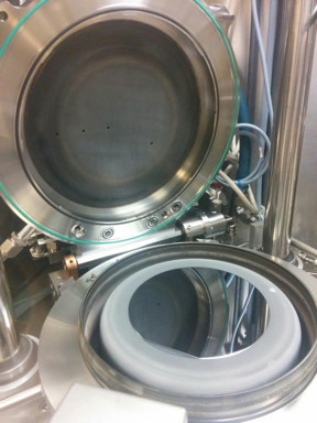 |
| The researchers used Micronova's cleanrooms and, in particular, a reactor designed for gallium nitride manufacturing. The image shows a six-inch substrate in the MOVPE reactor before manufacturing. CREDIT Aalto University / Jori Lemettinen |
Abstract:
In cooperation with Okmetic Oy and the Polish ITME, researchers at Aalto University have studied the application of SOI (Silicon On Insulator) wafers, which are used as a platform for manufacturing different microelectronics components, as a substrate for producing gallium nitride crystals. The researchers compared the characteristics of gallium nitride (GaN) layers grown on SOI wafers to those grown on silicon substrates more commonly used for the process. In addition to high-performance silicon wafers, Okmetic also manufactures SOI wafers, in which a layer of silicon dioxide insulator is sandwiched between two silicon layers. The objective of the SOI technology is to improve the capacitive and insulating characteristics of the wafer.
A SOI wafer is a suitable substrate for gallium nitride crystals: Improved characteristics in power electronics and radio applications can be achieved by using a SOI wafer for gallium nitride growth
Aalto, Finland | Posted on March 4th, 2017"We used a standardised manufacturing process for comparing the wafer characteristics. GaN growth on SOI wafers produced a higher crystalline quality layer than on silicon wafers. In addition, the insulating layer in the SOI wafer improves breakdown characteristics, enabling the use of clearly higher voltages in power electronics. Similarly, in high frequency applications, the losses and crosstalk can be reduced", explains Jori Lemettinen, a doctoral candidate from the Department of Electronics and Nanoengineering.
'GaN based components are becoming more common in power electronics and radio applications. The performance of GaN based devices can be improved by using a SOI wafer as the substrate', adds Academy Research Fellow Sami Suihkonen.
SOI wafers reduce the challenges of crystal growth
Growth of GaN on a silicon substrate is challenging. GaN layers and devices can be grown on substrate material using metalorganic vapor phase epitaxy (MOVPE). When using silicon as a substrate the grown compound semiconductor materials have different coefficients of thermal expansion and lattice constants than a silicon wafer. These differences in their characteristics limit the crystalline quality that can be achieved and the maximum possible thickness of the produced layer.
'The research showed that the layered structure of an SOI wafer can act as a compliant substrate during gallium nitride layer growth and thus reduce defects and strain in the grown layers", Lemettinen notes. GaN based components are commonly used in blue and white LEDs. In power electronics applications, GaN diodes and transistors, in particular, have received interest, for example in frequency converters or electric cars. It is believed that in radio applications, 5G network base stations will use GaN based power amplifiers in the future. In electronics applications, a GaN transistor offers low resistance and enables high frequencies and power densities.
#
####
For more information, please click here
Contacts:
Jori Lemettinen
358-405-723-087
Academy Research Fellow Sami Suihkonen
Aalto University
tel. +358 50 3618 657
Copyright © Aalto University
If you have a comment, please Contact us.Issuers of news releases, not 7th Wave, Inc. or Nanotechnology Now, are solely responsible for the accuracy of the content.
Bookmark:


| Related Links |
| Related News Press |
News and information
![]() Quantum computer improves AI predictions April 17th, 2026
Quantum computer improves AI predictions April 17th, 2026
![]() Flexible sensor gains sensitivity under pressure April 17th, 2026
Flexible sensor gains sensitivity under pressure April 17th, 2026
![]() A reusable chip for particulate matter sensing April 17th, 2026
A reusable chip for particulate matter sensing April 17th, 2026
![]() Detecting vibrational quantum beating in the predissociation dynamics of SF6 using time-resolved photoelectron spectroscopy April 17th, 2026
Detecting vibrational quantum beating in the predissociation dynamics of SF6 using time-resolved photoelectron spectroscopy April 17th, 2026
Hardware
![]() The present and future of computing get a boost from new research July 21st, 2023
The present and future of computing get a boost from new research July 21st, 2023
![]() A Carbon Nanotube Microprocessor Mature Enough to Say Hello: Three new breakthroughs make commercial nanotube processors possible March 2nd, 2020
A Carbon Nanotube Microprocessor Mature Enough to Say Hello: Three new breakthroughs make commercial nanotube processors possible March 2nd, 2020
![]() Powering the future: Smallest all-digital circuit opens doors to 5 nm next-gen semiconductor February 11th, 2020
Powering the future: Smallest all-digital circuit opens doors to 5 nm next-gen semiconductor February 11th, 2020
Possible Futures
![]() A fundamentally new therapeutic approach to cystic fibrosis: Nanobody repairs cellular defect April 17th, 2026
A fundamentally new therapeutic approach to cystic fibrosis: Nanobody repairs cellular defect April 17th, 2026
![]() UC Irvine physicists discover method to reverse �quantum scrambling� : The work addresses the problem of information loss in quantum computing system April 17th, 2026
UC Irvine physicists discover method to reverse �quantum scrambling� : The work addresses the problem of information loss in quantum computing system April 17th, 2026
Chip Technology
![]() A reusable chip for particulate matter sensing April 17th, 2026
A reusable chip for particulate matter sensing April 17th, 2026
![]() Metasurfaces smooth light to boost magnetic sensing precision January 30th, 2026
Metasurfaces smooth light to boost magnetic sensing precision January 30th, 2026
Nanoelectronics
![]() Lab to industry: InSe wafer-scale breakthrough for future electronics August 8th, 2025
Lab to industry: InSe wafer-scale breakthrough for future electronics August 8th, 2025
![]() Interdisciplinary: Rice team tackles the future of semiconductors Multiferroics could be the key to ultralow-energy computing October 6th, 2023
Interdisciplinary: Rice team tackles the future of semiconductors Multiferroics could be the key to ultralow-energy computing October 6th, 2023
![]() Key element for a scalable quantum computer: Physicists from Forschungszentrum J�lich and RWTH Aachen University demonstrate electron transport on a quantum chip September 23rd, 2022
Key element for a scalable quantum computer: Physicists from Forschungszentrum J�lich and RWTH Aachen University demonstrate electron transport on a quantum chip September 23rd, 2022
![]() Reduced power consumption in semiconductor devices September 23rd, 2022
Reduced power consumption in semiconductor devices September 23rd, 2022
Discoveries
![]() Quantum computer improves AI predictions April 17th, 2026
Quantum computer improves AI predictions April 17th, 2026
![]() Flexible sensor gains sensitivity under pressure April 17th, 2026
Flexible sensor gains sensitivity under pressure April 17th, 2026
![]() A reusable chip for particulate matter sensing April 17th, 2026
A reusable chip for particulate matter sensing April 17th, 2026
![]() Detecting vibrational quantum beating in the predissociation dynamics of SF6 using time-resolved photoelectron spectroscopy April 17th, 2026
Detecting vibrational quantum beating in the predissociation dynamics of SF6 using time-resolved photoelectron spectroscopy April 17th, 2026
Announcements
![]() A fundamentally new therapeutic approach to cystic fibrosis: Nanobody repairs cellular defect April 17th, 2026
A fundamentally new therapeutic approach to cystic fibrosis: Nanobody repairs cellular defect April 17th, 2026
![]() UC Irvine physicists discover method to reverse �quantum scrambling� : The work addresses the problem of information loss in quantum computing system April 17th, 2026
UC Irvine physicists discover method to reverse �quantum scrambling� : The work addresses the problem of information loss in quantum computing system April 17th, 2026
Interviews/Book Reviews/Essays/Reports/Podcasts/Journals/White papers/Posters
![]() A fundamentally new therapeutic approach to cystic fibrosis: Nanobody repairs cellular defect April 17th, 2026
A fundamentally new therapeutic approach to cystic fibrosis: Nanobody repairs cellular defect April 17th, 2026
![]() UC Irvine physicists discover method to reverse �quantum scrambling� : The work addresses the problem of information loss in quantum computing system April 17th, 2026
UC Irvine physicists discover method to reverse �quantum scrambling� : The work addresses the problem of information loss in quantum computing system April 17th, 2026
|
|
||
|
|
||
| The latest news from around the world, FREE | ||
|
|
||
|
|
||
| Premium Products | ||
|
|
||
|
Only the news you want to read!
Learn More |
||
|
|
||
|
Full-service, expert consulting
Learn More |
||
|
|
||