Home > Press > Semiconductor-free microelectronics are now possible, thanks to metamaterials
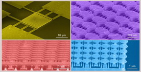 |
| These are scanning electron micrograph images of the semiconductor-free microelectronic device (top left) and the gold metasurface (top right, bottom). CREDIT UC San Diego Applied Electromagnetics Group |
Abstract:
Engineers at the University of California San Diego have fabricated the first semiconductor-free, optically-controlled microelectronic device. Using metamaterials, engineers were able to build a microscale device that shows a 1,000 percent increase in conductivity when activated by low voltage and a low power laser.
Semiconductor-free microelectronics are now possible, thanks to metamaterials
San Diego, CA | Posted on November 9th, 2016The discovery paves the way for microelectronic devices that are faster and capable of handling more power, and could also lead to more efficient solar panels. The work was published Nov. 4 in Nature Communications.
The capabilities of existing microelectronic devices, such as transistors, are ultimately limited by the properties of their constituent materials, such as their semiconductors, researchers said.
For example, semiconductors can impose limits on a device's conductivity, or electron flow. Semiconductors have what's called a band gap, meaning they require a boost of external energy to get electrons to flow through them. And electron velocity is limited, since electrons are constantly colliding with atoms as they flow through the semiconductor.
A team of researchers in the Applied Electromagnetics Group led by electrical engineering professor Dan Sievenpiper at UC San Diego sought to remove these roadblocks to conductivity by replacing semiconductors with free electrons in space. "And we wanted to do this at the microscale," said Ebrahim Forati, a former postdoctoral researcher in Sievenpiper's lab and first author of the study.
However, liberating electrons from materials is challenging. It either requires applying high voltages (at least 100 Volts), high power lasers or extremely high temperatures (more than 1,000 degrees Fahrenheit), which aren't practical in micro- and nanoscale electronic devices.
To address this challenge, Sievenpiper's team fabricated a microscale device that can release electrons from a material without such extreme requirements. The device consists of an engineered surface, called a metasurface, on top of a silicon wafer, with a layer of silicon dioxide in between. The metasurface consists of an array of gold mushroom-like nanostructures on an array of parallel gold strips.
The gold metasurface is designed such that when a low DC voltage (under 10 Volts) and a low power infrared laser are both applied, the metasurface generates "hot spots"--spots with a high intensity electric field--that provide enough energy to pull electrons out from the metal and liberate them into space.
Tests on the device showed a 1,000 percent change in conductivity. "That means more available electrons for manipulation," Ebrahim said.
"This certainly won't replace all semiconductor devices, but it may be the best approach for certain specialty applications, such as very high frequencies or high power devices," Sievenpiper said.
According to researchers, this particular metasurface was designed as a proof-of-concept. Different metasurfaces will need to be designed and optimized for different types of microelectronic devices.
"Next we need to understand how far these devices can be scaled and the limits of their performance," Sievenpiper said. The team is also exploring other applications for this technology besides electronics, such as photochemistry, photocatalysis, enabling new kinds of photovoltaic devices or environmental applications.
This work was funded by Defense Advanced Research Projects Agency (grant N00014-13-1-0618) and the Office of Naval Research Defense University Research Instrumentation Program (grant N00014-13-1-0655).
####
For more information, please click here
Contacts:
Liezel Labios
858-246-1124
Copyright © University of California, San Diego
If you have a comment, please Contact us.Issuers of news releases, not 7th Wave, Inc. or Nanotechnology Now, are solely responsible for the accuracy of the content.
Bookmark:


| Related Links |
| Related News Press |
News and information
![]() Quantum computer improves AI predictions April 17th, 2026
Quantum computer improves AI predictions April 17th, 2026
![]() Flexible sensor gains sensitivity under pressure April 17th, 2026
Flexible sensor gains sensitivity under pressure April 17th, 2026
![]() A reusable chip for particulate matter sensing April 17th, 2026
A reusable chip for particulate matter sensing April 17th, 2026
![]() Detecting vibrational quantum beating in the predissociation dynamics of SF6 using time-resolved photoelectron spectroscopy April 17th, 2026
Detecting vibrational quantum beating in the predissociation dynamics of SF6 using time-resolved photoelectron spectroscopy April 17th, 2026
Govt.-Legislation/Regulation/Funding/Policy
![]() Quantum computer improves AI predictions April 17th, 2026
Quantum computer improves AI predictions April 17th, 2026
![]() Metasurfaces smooth light to boost magnetic sensing precision January 30th, 2026
Metasurfaces smooth light to boost magnetic sensing precision January 30th, 2026
![]() New imaging approach transforms study of bacterial biofilms August 8th, 2025
New imaging approach transforms study of bacterial biofilms August 8th, 2025
Possible Futures
![]() A fundamentally new therapeutic approach to cystic fibrosis: Nanobody repairs cellular defect April 17th, 2026
A fundamentally new therapeutic approach to cystic fibrosis: Nanobody repairs cellular defect April 17th, 2026
![]() UC Irvine physicists discover method to reverse �quantum scrambling� : The work addresses the problem of information loss in quantum computing system April 17th, 2026
UC Irvine physicists discover method to reverse �quantum scrambling� : The work addresses the problem of information loss in quantum computing system April 17th, 2026
MEMS
Chip Technology
![]() A reusable chip for particulate matter sensing April 17th, 2026
A reusable chip for particulate matter sensing April 17th, 2026
![]() Metasurfaces smooth light to boost magnetic sensing precision January 30th, 2026
Metasurfaces smooth light to boost magnetic sensing precision January 30th, 2026
Optical computing/Photonic computing
![]() ICFO researchers overcome long-standing bottleneck in single photon detection with twisted 2D materials August 8th, 2025
ICFO researchers overcome long-standing bottleneck in single photon detection with twisted 2D materials August 8th, 2025
![]() Programmable electron-induced color router array May 14th, 2025
Programmable electron-induced color router array May 14th, 2025
Discoveries
![]() Quantum computer improves AI predictions April 17th, 2026
Quantum computer improves AI predictions April 17th, 2026
![]() Flexible sensor gains sensitivity under pressure April 17th, 2026
Flexible sensor gains sensitivity under pressure April 17th, 2026
![]() A reusable chip for particulate matter sensing April 17th, 2026
A reusable chip for particulate matter sensing April 17th, 2026
![]() Detecting vibrational quantum beating in the predissociation dynamics of SF6 using time-resolved photoelectron spectroscopy April 17th, 2026
Detecting vibrational quantum beating in the predissociation dynamics of SF6 using time-resolved photoelectron spectroscopy April 17th, 2026
Materials/Metamaterials/Magnetoresistance
![]() First real-time observation of two-dimensional melting process: Researchers at Mainz University unveil new insights into magnetic vortex structures August 8th, 2025
First real-time observation of two-dimensional melting process: Researchers at Mainz University unveil new insights into magnetic vortex structures August 8th, 2025
![]() Researchers unveil a groundbreaking clay-based solution to capture carbon dioxide and combat climate change June 6th, 2025
Researchers unveil a groundbreaking clay-based solution to capture carbon dioxide and combat climate change June 6th, 2025
![]() A 1960s idea inspires NBI researchers to study hitherto inaccessible quantum states June 6th, 2025
A 1960s idea inspires NBI researchers to study hitherto inaccessible quantum states June 6th, 2025
![]() Institute for Nanoscience hosts annual proposal planning meeting May 16th, 2025
Institute for Nanoscience hosts annual proposal planning meeting May 16th, 2025
Announcements
![]() A fundamentally new therapeutic approach to cystic fibrosis: Nanobody repairs cellular defect April 17th, 2026
A fundamentally new therapeutic approach to cystic fibrosis: Nanobody repairs cellular defect April 17th, 2026
![]() UC Irvine physicists discover method to reverse �quantum scrambling� : The work addresses the problem of information loss in quantum computing system April 17th, 2026
UC Irvine physicists discover method to reverse �quantum scrambling� : The work addresses the problem of information loss in quantum computing system April 17th, 2026
Interviews/Book Reviews/Essays/Reports/Podcasts/Journals/White papers/Posters
![]() A fundamentally new therapeutic approach to cystic fibrosis: Nanobody repairs cellular defect April 17th, 2026
A fundamentally new therapeutic approach to cystic fibrosis: Nanobody repairs cellular defect April 17th, 2026
![]() UC Irvine physicists discover method to reverse �quantum scrambling� : The work addresses the problem of information loss in quantum computing system April 17th, 2026
UC Irvine physicists discover method to reverse �quantum scrambling� : The work addresses the problem of information loss in quantum computing system April 17th, 2026
Military
![]() Quantum engineers �squeeze� laser frequency combs to make more sensitive gas sensors January 17th, 2025
Quantum engineers �squeeze� laser frequency combs to make more sensitive gas sensors January 17th, 2025
![]() Chainmail-like material could be the future of armor: First 2D mechanically interlocked polymer exhibits exceptional flexibility and strength January 17th, 2025
Chainmail-like material could be the future of armor: First 2D mechanically interlocked polymer exhibits exceptional flexibility and strength January 17th, 2025
![]() Single atoms show their true color July 5th, 2024
Single atoms show their true color July 5th, 2024
![]() NRL charters Navy�s quantum inertial navigation path to reduce drift April 5th, 2024
NRL charters Navy�s quantum inertial navigation path to reduce drift April 5th, 2024
Environment
![]() A reusable chip for particulate matter sensing April 17th, 2026
A reusable chip for particulate matter sensing April 17th, 2026
![]() Researchers unveil a groundbreaking clay-based solution to capture carbon dioxide and combat climate change June 6th, 2025
Researchers unveil a groundbreaking clay-based solution to capture carbon dioxide and combat climate change June 6th, 2025
Energy
![]() Sensors innovations for smart lithium-based batteries: advancements, opportunities, and potential challenges August 8th, 2025
Sensors innovations for smart lithium-based batteries: advancements, opportunities, and potential challenges August 8th, 2025
![]() Simple algorithm paired with standard imaging tool could predict failure in lithium metal batteries August 8th, 2025
Simple algorithm paired with standard imaging tool could predict failure in lithium metal batteries August 8th, 2025
Photonics/Optics/Lasers
![]() Metasurfaces smooth light to boost magnetic sensing precision January 30th, 2026
Metasurfaces smooth light to boost magnetic sensing precision January 30th, 2026
![]() From sensors to smart systems: the rise of AI-driven photonic noses January 30th, 2026
From sensors to smart systems: the rise of AI-driven photonic noses January 30th, 2026
|
|
||
|
|
||
| The latest news from around the world, FREE | ||
|
|
||
|
|
||
| Premium Products | ||
|
|
||
|
Only the news you want to read!
Learn More |
||
|
|
||
|
Full-service, expert consulting
Learn More |
||
|
|
||