Home > Press > Iowa State engineers treat printed graphene with lasers to enable paper electronics
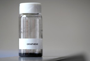 |
| Iowa State engineers are developing real-world, low-cost applications for graphene.
Photos by Christopher Gannon/Iowa State University. |
Abstract:
The researchers in Jonathan Claussen's lab at Iowa State University (who like to call themselves nanoengineers) have been looking for ways to use graphene and its amazing properties in their sensors and other technologies.
Iowa State engineers treat printed graphene with lasers to enable paper electronics
Ames, IA | Posted on September 2nd, 2016Graphene is a wonder material: The carbon honeycomb is just an atom thick. It's great at conducting electricity and heat; it's strong and stable. But researchers have struggled to move beyond tiny lab samples for studying its material properties to larger pieces for real-world applications.
Recent projects that used inkjet printers to print multi-layer graphene circuits and electrodes had the engineers thinking about using it for flexible, wearable and low-cost electronics. For example, "Could we make graphene at scales large enough for glucose sensors?" asked Suprem Das, an Iowa State postdoctoral research associate in mechanical engineering and an associate of the U.S. Department of Energy's Ames Laboratory.
But there were problems with the existing technology. Once printed, the graphene had to be treated to improve electrical conductivity and device performance. That usually meant high temperatures or chemicals - both could degrade flexible or disposable printing surfaces such as plastic films or even paper.
Das and Claussen came up with the idea of using lasers to treat the graphene. Claussen, an Iowa State assistant professor of mechanical engineering and an Ames Laboratory associate, worked with Gary Cheng, an associate professor at Purdue University's School of Industrial Engineering, to develop and test the idea.
And it worked: They found treating inkjet-printed, multi-layer graphene electric circuits and electrodes with a pulsed-laser process improves electrical conductivity without damaging paper, polymers or other fragile printing surfaces.
"This creates a way to commercialize and scale-up the manufacturing of graphene," Claussen said.
The findings are featured on the front cover of the journal Nanoscale's issue 35. Claussen and Cheng are lead authors and Das is first author. Additional Iowa State co-authors are Allison Cargill, John Hondred and Shaowei Ding, graduate students in mechanical engineering. Additional Purdue co-authors are Qiong Nian and Mojib Saei, graduate students in industrial engineering.
Two major grants are supporting the project and related research: a three-year grant from the National Institute of Food and Agriculture, U.S. Department of Agriculture, under award number 11901762 and a three-year grant from the Roy J. Carver Charitable Trust. Iowa State's College of Engineering and department of mechanical engineering are also supporting the research.
The Iowa State Research Foundation Inc. has filed for a patent on the technology.
"The breakthrough of this project is transforming the inkjet-printed graphene into a conductive material capable of being used in new applications," Claussen said.
Those applications could include sensors with biological applications, energy storage systems, electrical conducting components and even paper-based electronics.
To make all that possible, the engineers developed computer-controlled laser technology that selectively irradiates inkjet-printed graphene oxide. The treatment removes ink binders and reduces graphene oxide to graphene - physically stitching together millions of tiny graphene flakes. The process makes electrical conductivity more than a thousand times better.
"The laser works with a rapid pulse of high-energy photons that do not destroy the graphene or the substrate," Das said. "They heat locally. They bombard locally. They process locally."
That localized, laser processing also changes the shape and structure of the printed graphene from a flat surface to one with raised, 3-D nanostructures. The engineers say the 3-D structures are like tiny petals rising from the surface. The rough and ridged structure increases the electrochemical reactivity of the graphene, making it useful for chemical and biological sensors.
All of that, according to Claussen's team of nanoengineers, could move graphene to commercial applications.
"This work paves the way for not only paper-based electronics with graphene circuits," the researchers wrote in their paper, "it enables the creation of low-cost and disposable graphene-based electrochemical electrodes for myriad applications including sensors, biosensors, fuel cells and (medical) devices."
####
For more information, please click here
Contacts:
Jonathan Claussen
515-294-4690
Copyright © Iowa State University
If you have a comment, please Contact us.Issuers of news releases, not 7th Wave, Inc. or Nanotechnology Now, are solely responsible for the accuracy of the content.
Bookmark:


| Related Links |
| Related News Press |
News and information
![]() Quantum computer improves AI predictions April 17th, 2026
Quantum computer improves AI predictions April 17th, 2026
![]() Flexible sensor gains sensitivity under pressure April 17th, 2026
Flexible sensor gains sensitivity under pressure April 17th, 2026
![]() A reusable chip for particulate matter sensing April 17th, 2026
A reusable chip for particulate matter sensing April 17th, 2026
![]() Detecting vibrational quantum beating in the predissociation dynamics of SF6 using time-resolved photoelectron spectroscopy April 17th, 2026
Detecting vibrational quantum beating in the predissociation dynamics of SF6 using time-resolved photoelectron spectroscopy April 17th, 2026
2 Dimensional Materials
![]() Flexible sensor gains sensitivity under pressure April 17th, 2026
Flexible sensor gains sensitivity under pressure April 17th, 2026
Graphene/ Graphite
![]() Electrifying results shed light on graphene foam as a potential material for lab grown cartilage June 6th, 2025
Electrifying results shed light on graphene foam as a potential material for lab grown cartilage June 6th, 2025
![]() Breakthrough in proton barrier films using pore-free graphene oxide: Kumamoto University researchers achieve new milestone in advanced coating technologies September 13th, 2024
Breakthrough in proton barrier films using pore-free graphene oxide: Kumamoto University researchers achieve new milestone in advanced coating technologies September 13th, 2024
Possible Futures
![]() A fundamentally new therapeutic approach to cystic fibrosis: Nanobody repairs cellular defect April 17th, 2026
A fundamentally new therapeutic approach to cystic fibrosis: Nanobody repairs cellular defect April 17th, 2026
![]() UC Irvine physicists discover method to reverse �quantum scrambling� : The work addresses the problem of information loss in quantum computing system April 17th, 2026
UC Irvine physicists discover method to reverse �quantum scrambling� : The work addresses the problem of information loss in quantum computing system April 17th, 2026
Chip Technology
![]() A reusable chip for particulate matter sensing April 17th, 2026
A reusable chip for particulate matter sensing April 17th, 2026
![]() Metasurfaces smooth light to boost magnetic sensing precision January 30th, 2026
Metasurfaces smooth light to boost magnetic sensing precision January 30th, 2026
Nanomedicine
![]() A fundamentally new therapeutic approach to cystic fibrosis: Nanobody repairs cellular defect April 17th, 2026
A fundamentally new therapeutic approach to cystic fibrosis: Nanobody repairs cellular defect April 17th, 2026
![]() New molecular technology targets tumors and simultaneously silences two �undruggable� cancer genes August 8th, 2025
New molecular technology targets tumors and simultaneously silences two �undruggable� cancer genes August 8th, 2025
![]() New imaging approach transforms study of bacterial biofilms August 8th, 2025
New imaging approach transforms study of bacterial biofilms August 8th, 2025
![]() Electrifying results shed light on graphene foam as a potential material for lab grown cartilage June 6th, 2025
Electrifying results shed light on graphene foam as a potential material for lab grown cartilage June 6th, 2025
Sensors
![]() Flexible sensor gains sensitivity under pressure April 17th, 2026
Flexible sensor gains sensitivity under pressure April 17th, 2026
![]() Tiny nanosheets, big leap: A new sensor detects ethanol at ultra-low levels January 30th, 2026
Tiny nanosheets, big leap: A new sensor detects ethanol at ultra-low levels January 30th, 2026
![]() From sensors to smart systems: the rise of AI-driven photonic noses January 30th, 2026
From sensors to smart systems: the rise of AI-driven photonic noses January 30th, 2026
![]() Sensors innovations for smart lithium-based batteries: advancements, opportunities, and potential challenges August 8th, 2025
Sensors innovations for smart lithium-based batteries: advancements, opportunities, and potential challenges August 8th, 2025
Discoveries
![]() Quantum computer improves AI predictions April 17th, 2026
Quantum computer improves AI predictions April 17th, 2026
![]() Flexible sensor gains sensitivity under pressure April 17th, 2026
Flexible sensor gains sensitivity under pressure April 17th, 2026
![]() A reusable chip for particulate matter sensing April 17th, 2026
A reusable chip for particulate matter sensing April 17th, 2026
![]() Detecting vibrational quantum beating in the predissociation dynamics of SF6 using time-resolved photoelectron spectroscopy April 17th, 2026
Detecting vibrational quantum beating in the predissociation dynamics of SF6 using time-resolved photoelectron spectroscopy April 17th, 2026
Announcements
![]() A fundamentally new therapeutic approach to cystic fibrosis: Nanobody repairs cellular defect April 17th, 2026
A fundamentally new therapeutic approach to cystic fibrosis: Nanobody repairs cellular defect April 17th, 2026
![]() UC Irvine physicists discover method to reverse �quantum scrambling� : The work addresses the problem of information loss in quantum computing system April 17th, 2026
UC Irvine physicists discover method to reverse �quantum scrambling� : The work addresses the problem of information loss in quantum computing system April 17th, 2026
Interviews/Book Reviews/Essays/Reports/Podcasts/Journals/White papers/Posters
![]() A fundamentally new therapeutic approach to cystic fibrosis: Nanobody repairs cellular defect April 17th, 2026
A fundamentally new therapeutic approach to cystic fibrosis: Nanobody repairs cellular defect April 17th, 2026
![]() UC Irvine physicists discover method to reverse �quantum scrambling� : The work addresses the problem of information loss in quantum computing system April 17th, 2026
UC Irvine physicists discover method to reverse �quantum scrambling� : The work addresses the problem of information loss in quantum computing system April 17th, 2026
Fuel Cells
![]() Deciphering local microstrain-induced optimization of asymmetric Fe single atomic sites for efficient oxygen reduction August 8th, 2025
Deciphering local microstrain-induced optimization of asymmetric Fe single atomic sites for efficient oxygen reduction August 8th, 2025
![]() Current and Future Developments in Nanomaterials and Carbon Nanotubes: Applications of Nanomaterials in Energy Storage and Electronics October 28th, 2022
Current and Future Developments in Nanomaterials and Carbon Nanotubes: Applications of Nanomaterials in Energy Storage and Electronics October 28th, 2022
|
|
||
|
|
||
| The latest news from around the world, FREE | ||
|
|
||
|
|
||
| Premium Products | ||
|
|
||
|
Only the news you want to read!
Learn More |
||
|
|
||
|
Full-service, expert consulting
Learn More |
||
|
|
||