Home > Press > Graphene key to growing 2-dimensional semiconductor with extraordinary properties
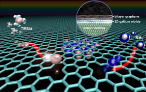 |
| This is an illustration of the Migration Enhance Encapsulated Growth (MEEG) process to stabilize novel wide-bandgap two-dimensional nitride semiconductors that are not naturally occurring. MEEG is facilitated by defects in the graphene lattice that act as pathways for intercalation. When the gallium and nitrogen adatoms meet at the graphene/SiC interface, they chemically react to form two-dimensional gallium nitride.
CREDIT: Z. Al Balushi and Stephen Weitzner, Penn State MatSE |
Abstract:
A newly discovered method for making two-dimensional materials could lead to new and extraordinary properties, particularly in a class of materials called nitrides, say the Penn State materials scientists who discovered the process. This first-ever growth of two-dimensional gallium nitride using graphene encapsulation could lead to applications in deep ultraviolet lasers, next-generation electronics and sensors.
Graphene key to growing 2-dimensional semiconductor with extraordinary properties
University Park, PA | Posted on August 30th, 2016"These experimental results open up new avenues of research in 2D materials," says Joshua Robinson, associate professor of materials science and engineering. "This work focuses on making 2D gallium nitride, which has never been done before."
Gallium nitride in its three-dimensional form is known to be a wide-bandgap semiconductor. Wide-bandgap semiconductors are important for high frequency, high power applications. When grown in its two-dimensional form, gallium nitride transforms from a wide-bandgap material to an ultrawide-bandgap material, effectively tripling the energy spectrum it can operate in, including the whole ultraviolet, visible and infrared spectrum. This work will have a particular impact on electro-optic devices that manipulate and transmit light.
"This is a new way of thinking about synthesizing 2D materials," said Zak Al Balushi, a Ph.D. candidate coadvised by Robinson and Joan Redwing, professor of materials science and engineering and electrical engineering. Al Balushi is lead author on a paper appearing online today (Aug.29) in the journal Nature Materials titled "Two-Dimensional Gallium Nitride Realized via Graphene Encapsulation."
"We have this palette of naturally occurring 2D materials," he continued. "But to expand beyond this, we have to synthesize materials that do not exist in nature. Typically, new material systems are highly unstable. But our growth method, called Migration Enhanced Encapsulated Growth (MEEG), uses a layer of graphene to assist the growth and stabilize a robust structure of 2D gallium nitride."
The graphene is grown on a substrate of silicon carbide, which is a technologically important substrate used widely in industry for LEDs, radar and telecommunications. When heated, the silicon on the surface decomposes and leaves a carbon-rich surface that can reconstruct into graphene. The advantage of producing the graphene in this way is that the interface where the two materials meet is perfectly smooth.
Robinson believes that in the case of two-dimensional gallium nitride, the addition of a layer of graphene makes all the difference. Graphene, a one-atom-thick layer of carbon atoms, is known for its remarkable electronic properties and strength.
"It's the key," Robinson says. "If you try to grow these materials the traditional way, on silicon carbide, you normally just form islands. It doesn't grow in nice layers on the silicon carbide."
When gallium atoms are added to the mix, they migrate through the graphene and form the middle layer of a sandwich, with graphene floating on top. When nitrogen atoms are added, a chemical reaction takes place that turns the gallium and nitrogen into gallium nitride.
"The MEEG process not only produces ultra-thin sheets of gallium nitride but also changes the crystal structure of the material, which may lead to entirely new applications in electronics and optoelectronics," said Redwing.
###
Additional coauthors include Ke Wang, Rafael Vila, Sarah Eichfield, Yu-Chuan Lin and Shruti Subramanian of Penn State, Ram Krishna Ghosh and Suman Datta of Notre Dame, Joshua Caldwell, U.S. Naval Research Laboratory, Xiaoye Qin and Robert Wallace The University of Texas at Dallas and Dennis Paul, Physical Electronics USA.
The Asahi Glass Co., Ltd, Japan, and the U.S. National Science Foundation provided funding for this project. The NSF Materials Science and Engineering Center at Penn State provided funding for Al Balushi. Other funding was provided by the Alfred P. Sloan Foundation, the Penn State Materials Characterization Laboratory and the Center for Low Energy Systems Technology (LEAST), funded by the Semiconductor Research Corporation and DARPA.
####
For more information, please click here
Contacts:
A'ndrea Elyse Messer
814-865-9481
Copyright © Penn State
If you have a comment, please Contact us.Issuers of news releases, not 7th Wave, Inc. or Nanotechnology Now, are solely responsible for the accuracy of the content.
Bookmark:


| Related Links |
| Related News Press |
News and information
![]() Quantum computer improves AI predictions April 17th, 2026
Quantum computer improves AI predictions April 17th, 2026
![]() Flexible sensor gains sensitivity under pressure April 17th, 2026
Flexible sensor gains sensitivity under pressure April 17th, 2026
![]() A reusable chip for particulate matter sensing April 17th, 2026
A reusable chip for particulate matter sensing April 17th, 2026
![]() Detecting vibrational quantum beating in the predissociation dynamics of SF6 using time-resolved photoelectron spectroscopy April 17th, 2026
Detecting vibrational quantum beating in the predissociation dynamics of SF6 using time-resolved photoelectron spectroscopy April 17th, 2026
2 Dimensional Materials
![]() Flexible sensor gains sensitivity under pressure April 17th, 2026
Flexible sensor gains sensitivity under pressure April 17th, 2026
Govt.-Legislation/Regulation/Funding/Policy
![]() Quantum computer improves AI predictions April 17th, 2026
Quantum computer improves AI predictions April 17th, 2026
![]() Metasurfaces smooth light to boost magnetic sensing precision January 30th, 2026
Metasurfaces smooth light to boost magnetic sensing precision January 30th, 2026
![]() New imaging approach transforms study of bacterial biofilms August 8th, 2025
New imaging approach transforms study of bacterial biofilms August 8th, 2025
Possible Futures
![]() A fundamentally new therapeutic approach to cystic fibrosis: Nanobody repairs cellular defect April 17th, 2026
A fundamentally new therapeutic approach to cystic fibrosis: Nanobody repairs cellular defect April 17th, 2026
![]() UC Irvine physicists discover method to reverse �quantum scrambling� : The work addresses the problem of information loss in quantum computing system April 17th, 2026
UC Irvine physicists discover method to reverse �quantum scrambling� : The work addresses the problem of information loss in quantum computing system April 17th, 2026
Chip Technology
![]() A reusable chip for particulate matter sensing April 17th, 2026
A reusable chip for particulate matter sensing April 17th, 2026
![]() Metasurfaces smooth light to boost magnetic sensing precision January 30th, 2026
Metasurfaces smooth light to boost magnetic sensing precision January 30th, 2026
Sensors
![]() Flexible sensor gains sensitivity under pressure April 17th, 2026
Flexible sensor gains sensitivity under pressure April 17th, 2026
![]() Tiny nanosheets, big leap: A new sensor detects ethanol at ultra-low levels January 30th, 2026
Tiny nanosheets, big leap: A new sensor detects ethanol at ultra-low levels January 30th, 2026
![]() From sensors to smart systems: the rise of AI-driven photonic noses January 30th, 2026
From sensors to smart systems: the rise of AI-driven photonic noses January 30th, 2026
![]() Sensors innovations for smart lithium-based batteries: advancements, opportunities, and potential challenges August 8th, 2025
Sensors innovations for smart lithium-based batteries: advancements, opportunities, and potential challenges August 8th, 2025
Nanoelectronics
![]() Lab to industry: InSe wafer-scale breakthrough for future electronics August 8th, 2025
Lab to industry: InSe wafer-scale breakthrough for future electronics August 8th, 2025
![]() Interdisciplinary: Rice team tackles the future of semiconductors Multiferroics could be the key to ultralow-energy computing October 6th, 2023
Interdisciplinary: Rice team tackles the future of semiconductors Multiferroics could be the key to ultralow-energy computing October 6th, 2023
![]() Key element for a scalable quantum computer: Physicists from Forschungszentrum J�lich and RWTH Aachen University demonstrate electron transport on a quantum chip September 23rd, 2022
Key element for a scalable quantum computer: Physicists from Forschungszentrum J�lich and RWTH Aachen University demonstrate electron transport on a quantum chip September 23rd, 2022
![]() Reduced power consumption in semiconductor devices September 23rd, 2022
Reduced power consumption in semiconductor devices September 23rd, 2022
Discoveries
![]() Quantum computer improves AI predictions April 17th, 2026
Quantum computer improves AI predictions April 17th, 2026
![]() Flexible sensor gains sensitivity under pressure April 17th, 2026
Flexible sensor gains sensitivity under pressure April 17th, 2026
![]() A reusable chip for particulate matter sensing April 17th, 2026
A reusable chip for particulate matter sensing April 17th, 2026
![]() Detecting vibrational quantum beating in the predissociation dynamics of SF6 using time-resolved photoelectron spectroscopy April 17th, 2026
Detecting vibrational quantum beating in the predissociation dynamics of SF6 using time-resolved photoelectron spectroscopy April 17th, 2026
Materials/Metamaterials/Magnetoresistance
![]() First real-time observation of two-dimensional melting process: Researchers at Mainz University unveil new insights into magnetic vortex structures August 8th, 2025
First real-time observation of two-dimensional melting process: Researchers at Mainz University unveil new insights into magnetic vortex structures August 8th, 2025
![]() Researchers unveil a groundbreaking clay-based solution to capture carbon dioxide and combat climate change June 6th, 2025
Researchers unveil a groundbreaking clay-based solution to capture carbon dioxide and combat climate change June 6th, 2025
![]() A 1960s idea inspires NBI researchers to study hitherto inaccessible quantum states June 6th, 2025
A 1960s idea inspires NBI researchers to study hitherto inaccessible quantum states June 6th, 2025
![]() Institute for Nanoscience hosts annual proposal planning meeting May 16th, 2025
Institute for Nanoscience hosts annual proposal planning meeting May 16th, 2025
Announcements
![]() A fundamentally new therapeutic approach to cystic fibrosis: Nanobody repairs cellular defect April 17th, 2026
A fundamentally new therapeutic approach to cystic fibrosis: Nanobody repairs cellular defect April 17th, 2026
![]() UC Irvine physicists discover method to reverse �quantum scrambling� : The work addresses the problem of information loss in quantum computing system April 17th, 2026
UC Irvine physicists discover method to reverse �quantum scrambling� : The work addresses the problem of information loss in quantum computing system April 17th, 2026
Military
![]() Quantum engineers �squeeze� laser frequency combs to make more sensitive gas sensors January 17th, 2025
Quantum engineers �squeeze� laser frequency combs to make more sensitive gas sensors January 17th, 2025
![]() Chainmail-like material could be the future of armor: First 2D mechanically interlocked polymer exhibits exceptional flexibility and strength January 17th, 2025
Chainmail-like material could be the future of armor: First 2D mechanically interlocked polymer exhibits exceptional flexibility and strength January 17th, 2025
![]() Single atoms show their true color July 5th, 2024
Single atoms show their true color July 5th, 2024
![]() NRL charters Navy�s quantum inertial navigation path to reduce drift April 5th, 2024
NRL charters Navy�s quantum inertial navigation path to reduce drift April 5th, 2024
Grants/Sponsored Research/Awards/Scholarships/Gifts/Contests/Honors/Records
![]() Quantum computer improves AI predictions April 17th, 2026
Quantum computer improves AI predictions April 17th, 2026
![]() Detecting vibrational quantum beating in the predissociation dynamics of SF6 using time-resolved photoelectron spectroscopy April 17th, 2026
Detecting vibrational quantum beating in the predissociation dynamics of SF6 using time-resolved photoelectron spectroscopy April 17th, 2026
![]() Metasurfaces smooth light to boost magnetic sensing precision January 30th, 2026
Metasurfaces smooth light to boost magnetic sensing precision January 30th, 2026
Photonics/Optics/Lasers
![]() Metasurfaces smooth light to boost magnetic sensing precision January 30th, 2026
Metasurfaces smooth light to boost magnetic sensing precision January 30th, 2026
![]() From sensors to smart systems: the rise of AI-driven photonic noses January 30th, 2026
From sensors to smart systems: the rise of AI-driven photonic noses January 30th, 2026
|
|
||
|
|
||
| The latest news from around the world, FREE | ||
|
|
||
|
|
||
| Premium Products | ||
|
|
||
|
Only the news you want to read!
Learn More |
||
|
|
||
|
Full-service, expert consulting
Learn More |
||
|
|
||