Home > Press > New microwave imaging approach opens a nanoscale view on processes in liquids: Technique can explore technologically and medically important processes that occur at boundaries between liquids and solids, such as in batteries or along cell membranes
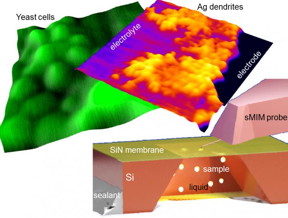 |
| NIST and ORNL scientists have devised a near-field microwave imaging approach to capture images of nanoscale processes under natural conditions. As the tip of an atomic force microscope scans over an ultrathin membrane it emits near-field microwaves into the sample below. Shown are images of yeast cells and silver dendrites, which formed on an electrode during electroplating. CREDIT: Kolmakov/CNST |
Abstract:
U.S. government nanotechnology researchers have demonstrated a new window to view what are now mostly clandestine operations occurring in soggy, inhospitable realms of the nanoworld--technologically and medically important processes that occur at boundaries between liquids and solids, such as in batteries or along cell membranes.
New microwave imaging approach opens a nanoscale view on processes in liquids: Technique can explore technologically and medically important processes that occur at boundaries between liquids and solids, such as in batteries or along cell membranes
Gaithersburg, MD | Posted on March 16th, 2016The new microwave imaging approach trumps X-ray and electron-based methods that can damage delicate samples and muddy results. And it spares expensive equipment from being exposed to liquids, while eliminating the need to harden probes against corrosive, toxic, or other harmful environments.
Writing in the journal ACS Nano, the collaborators--from the Center for Nanoscale Science and Technology at the National Institute of Standards and Technology (NIST) and the Department of Energy's Oak Ridge National Laboratory (ORNL)--describe their new approach to imaging reactive and biological samples at nanoscale levels under realistic conditions.
The key element is a window, an ultrathin membrane that separates the needle-like probe of an atomic force microscope (AFM) from the underlying sample, held in tiny containers that maintain a consistent liquid or gas environment. The addition transforms near-field microwave imaging into a versatile tool, extending its use beyond semiconductor technology, where it is used to study solid structures, to a new realm of liquids and gases.
"The ultrathin, microwave-transparent membrane allows the sample to be examined in much the same way that Earth's radar was used to reveal images of the surface of Venus through its opaque atmosphere," explained NIST physicist Andrei Kolmakov.
"We generate microwaves at the apex--or very end--of the probe tip," Kolmakov said. "The microwaves penetrate through the membrane a few hundred nanometers deep into the liquid up to the object of interest. As the tip scans the sample from across the membrane, we record the reflected microwaves to generate the image."
Microwaves are much larger than the nanoscale objects they are used to "seeing." But when emitted from only a minuscule distance away, near-field microwaves reflected from a sample yield a surprisingly detailed image.
In their proof-of-concept experiments, the NIST-ORNL team used their hybrid microscope to get a nanoscale view of the early stages of a silver electroplating process. Microwave images captured the electrochemical formation of branching metal clusters, or dendrites, on electrodes. Features nearly as small as 100 nanometers (billionths of a meter) could be discerned.
As important, the low-energy microwaves were too feeble to sever chemical bonds, heat, or interfere in other ways with the process they were being used to capture in images. In contrast, a scanning electron microscope that was used to record the same electroplating process at comparable levels of resolution yielded images showing delamination and other destructive effects of the electron beam.
The team reports similar success in using their AFM-microwave set-up to record images of yeast cells dispersed in water or glycerol. Levels of spatial resolution were comparable to those achieved with a scanning electron microscope, but again, were free of the damage caused by the electron beam.
In their experiments, the team used membranes--made either of silicon dioxide or silicon nitride--that ranged in thickness from 8 nanometers to 50 nanometers. They found, however, that the thinner the membrane the better the resolution--down to tens of nanometers--and the greater the probing depth--up to hundreds of nanometers.
"These numbers can be improved further with tuning and development of better electronics," Kolmakov said.
In addition to studying processes in reactive, toxic, or radioactive environments, the researchers suggest that their microwave-imaging approach might be integrated into "lab-on-a-chip" fluidic devices, where it can be used to sample liquids and gases.
###
The research was performed at NIST's Center for Nanoscale Science and Technology and at the Center for Nanophase Materials Sciences, a Department of Energy Office of Science User Facility.
####
For more information, please click here
Contacts:
Mark Bello
301-975-3776
Copyright © National Institute of Standards and Technology (NIST)
If you have a comment, please Contact us.Issuers of news releases, not 7th Wave, Inc. or Nanotechnology Now, are solely responsible for the accuracy of the content.
Bookmark:


| Related Links |
| Related News Press |
News and information
![]() Quantum computer improves AI predictions April 17th, 2026
Quantum computer improves AI predictions April 17th, 2026
![]() Flexible sensor gains sensitivity under pressure April 17th, 2026
Flexible sensor gains sensitivity under pressure April 17th, 2026
![]() A reusable chip for particulate matter sensing April 17th, 2026
A reusable chip for particulate matter sensing April 17th, 2026
![]() Detecting vibrational quantum beating in the predissociation dynamics of SF6 using time-resolved photoelectron spectroscopy April 17th, 2026
Detecting vibrational quantum beating in the predissociation dynamics of SF6 using time-resolved photoelectron spectroscopy April 17th, 2026
Imaging
![]() Simple algorithm paired with standard imaging tool could predict failure in lithium metal batteries August 8th, 2025
Simple algorithm paired with standard imaging tool could predict failure in lithium metal batteries August 8th, 2025
![]() First real-time observation of two-dimensional melting process: Researchers at Mainz University unveil new insights into magnetic vortex structures August 8th, 2025
First real-time observation of two-dimensional melting process: Researchers at Mainz University unveil new insights into magnetic vortex structures August 8th, 2025
![]() New imaging approach transforms study of bacterial biofilms August 8th, 2025
New imaging approach transforms study of bacterial biofilms August 8th, 2025
Microfluidics/Nanofluidics
![]() Projecting light to dispense liquids: A new route to ultra-precise microdroplets January 30th, 2026
Projecting light to dispense liquids: A new route to ultra-precise microdroplets January 30th, 2026
Laboratories
![]() Researchers develop molecular qubits that communicate at telecom frequencies October 3rd, 2025
Researchers develop molecular qubits that communicate at telecom frequencies October 3rd, 2025
Lab-on-a-chip
![]() Micro-scale opto-thermo-mechanical actuation in the dry adhesive regime Peer-Reviewed Publication September 24th, 2021
Micro-scale opto-thermo-mechanical actuation in the dry adhesive regime Peer-Reviewed Publication September 24th, 2021
![]() Silicon-graphene hybrid plasmonic waveguide photodetectors beyond 1.55 μm March 13th, 2020
Silicon-graphene hybrid plasmonic waveguide photodetectors beyond 1.55 μm March 13th, 2020
Govt.-Legislation/Regulation/Funding/Policy
![]() Quantum computer improves AI predictions April 17th, 2026
Quantum computer improves AI predictions April 17th, 2026
![]() Metasurfaces smooth light to boost magnetic sensing precision January 30th, 2026
Metasurfaces smooth light to boost magnetic sensing precision January 30th, 2026
![]() New imaging approach transforms study of bacterial biofilms August 8th, 2025
New imaging approach transforms study of bacterial biofilms August 8th, 2025
Possible Futures
![]() A fundamentally new therapeutic approach to cystic fibrosis: Nanobody repairs cellular defect April 17th, 2026
A fundamentally new therapeutic approach to cystic fibrosis: Nanobody repairs cellular defect April 17th, 2026
![]() UC Irvine physicists discover method to reverse �quantum scrambling� : The work addresses the problem of information loss in quantum computing system April 17th, 2026
UC Irvine physicists discover method to reverse �quantum scrambling� : The work addresses the problem of information loss in quantum computing system April 17th, 2026
Nanomedicine
![]() A fundamentally new therapeutic approach to cystic fibrosis: Nanobody repairs cellular defect April 17th, 2026
A fundamentally new therapeutic approach to cystic fibrosis: Nanobody repairs cellular defect April 17th, 2026
![]() New molecular technology targets tumors and simultaneously silences two �undruggable� cancer genes August 8th, 2025
New molecular technology targets tumors and simultaneously silences two �undruggable� cancer genes August 8th, 2025
![]() New imaging approach transforms study of bacterial biofilms August 8th, 2025
New imaging approach transforms study of bacterial biofilms August 8th, 2025
![]() Electrifying results shed light on graphene foam as a potential material for lab grown cartilage June 6th, 2025
Electrifying results shed light on graphene foam as a potential material for lab grown cartilage June 6th, 2025
Discoveries
![]() Quantum computer improves AI predictions April 17th, 2026
Quantum computer improves AI predictions April 17th, 2026
![]() Flexible sensor gains sensitivity under pressure April 17th, 2026
Flexible sensor gains sensitivity under pressure April 17th, 2026
![]() A reusable chip for particulate matter sensing April 17th, 2026
A reusable chip for particulate matter sensing April 17th, 2026
![]() Detecting vibrational quantum beating in the predissociation dynamics of SF6 using time-resolved photoelectron spectroscopy April 17th, 2026
Detecting vibrational quantum beating in the predissociation dynamics of SF6 using time-resolved photoelectron spectroscopy April 17th, 2026
Announcements
![]() A fundamentally new therapeutic approach to cystic fibrosis: Nanobody repairs cellular defect April 17th, 2026
A fundamentally new therapeutic approach to cystic fibrosis: Nanobody repairs cellular defect April 17th, 2026
![]() UC Irvine physicists discover method to reverse �quantum scrambling� : The work addresses the problem of information loss in quantum computing system April 17th, 2026
UC Irvine physicists discover method to reverse �quantum scrambling� : The work addresses the problem of information loss in quantum computing system April 17th, 2026
Interviews/Book Reviews/Essays/Reports/Podcasts/Journals/White papers/Posters
![]() A fundamentally new therapeutic approach to cystic fibrosis: Nanobody repairs cellular defect April 17th, 2026
A fundamentally new therapeutic approach to cystic fibrosis: Nanobody repairs cellular defect April 17th, 2026
![]() UC Irvine physicists discover method to reverse �quantum scrambling� : The work addresses the problem of information loss in quantum computing system April 17th, 2026
UC Irvine physicists discover method to reverse �quantum scrambling� : The work addresses the problem of information loss in quantum computing system April 17th, 2026
Tools
![]() Metasurfaces smooth light to boost magnetic sensing precision January 30th, 2026
Metasurfaces smooth light to boost magnetic sensing precision January 30th, 2026
![]() From sensors to smart systems: the rise of AI-driven photonic noses January 30th, 2026
From sensors to smart systems: the rise of AI-driven photonic noses January 30th, 2026
![]() Japan launches fully domestically produced quantum computer: Expo visitors to experience quantum computing firsthand August 8th, 2025
Japan launches fully domestically produced quantum computer: Expo visitors to experience quantum computing firsthand August 8th, 2025
Energy
![]() Sensors innovations for smart lithium-based batteries: advancements, opportunities, and potential challenges August 8th, 2025
Sensors innovations for smart lithium-based batteries: advancements, opportunities, and potential challenges August 8th, 2025
![]() Simple algorithm paired with standard imaging tool could predict failure in lithium metal batteries August 8th, 2025
Simple algorithm paired with standard imaging tool could predict failure in lithium metal batteries August 8th, 2025
Battery Technology/Capacitors/Generators/Piezoelectrics/Thermoelectrics/Energy storage
![]() Decoding hydrogen‑bond network of electrolyte for cryogenic durable aqueous zinc‑ion batteries January 30th, 2026
Decoding hydrogen‑bond network of electrolyte for cryogenic durable aqueous zinc‑ion batteries January 30th, 2026
![]() COF scaffold membrane with gate‑lane nanostructure for efficient Li+/Mg2+ separation January 30th, 2026
COF scaffold membrane with gate‑lane nanostructure for efficient Li+/Mg2+ separation January 30th, 2026
![]() MXene nanomaterials enter a new dimension Multilayer nanomaterial: MXene flakes created at Drexel University show new promise as 1D scrolls January 30th, 2026
MXene nanomaterials enter a new dimension Multilayer nanomaterial: MXene flakes created at Drexel University show new promise as 1D scrolls January 30th, 2026
Nanobiotechnology
![]() A fundamentally new therapeutic approach to cystic fibrosis: Nanobody repairs cellular defect April 17th, 2026
A fundamentally new therapeutic approach to cystic fibrosis: Nanobody repairs cellular defect April 17th, 2026
![]() New molecular technology targets tumors and simultaneously silences two �undruggable� cancer genes August 8th, 2025
New molecular technology targets tumors and simultaneously silences two �undruggable� cancer genes August 8th, 2025
![]() New imaging approach transforms study of bacterial biofilms August 8th, 2025
New imaging approach transforms study of bacterial biofilms August 8th, 2025
![]() Electrifying results shed light on graphene foam as a potential material for lab grown cartilage June 6th, 2025
Electrifying results shed light on graphene foam as a potential material for lab grown cartilage June 6th, 2025
|
|
||
|
|
||
| The latest news from around the world, FREE | ||
|
|
||
|
|
||
| Premium Products | ||
|
|
||
|
Only the news you want to read!
Learn More |
||
|
|
||
|
Full-service, expert consulting
Learn More |
||
|
|
||