Home > Press > 'Tuning in' to a fast and optimized internet: A new filter with the widest tuning span ever demonstrated on a silicon chip could help provide the low-cost flexibility needed for the next generation of high-speed optical networks
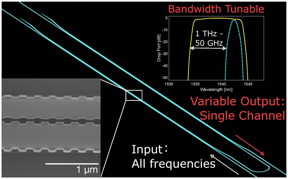 |
| The bandwidth-tunable silicon filter uses periodic nanostructures to filter a single channel from all input frequencies. The filter has the widest tuning span ever demonstrated on a silicon chip. CREDIT: Research Contact: Wei Shi Universit� Laval in Qu�bec, Canada wei.shi@gel.ulaval.ca |
Abstract:
The amount of data that flows over the internet has exploded in the last decade. Whether people are watching cat videos, streaming movies, or uploading vacation photos to social media sites, they are demanding ever higher performance from the optical networks that are the physical foundation of the World Wide Web.
'Tuning in' to a fast and optimized internet: A new filter with the widest tuning span ever demonstrated on a silicon chip could help provide the low-cost flexibility needed for the next generation of high-speed optical networks
Washington, DC | Posted on November 18th, 2015Yet the path toward an even faster internet has been hindered by energy consumption and cost per optical component, said Wei Shi, Assistant Professor, Universit� Laval in Qu�bec, Canada. Shi and his colleagues have designed a tunable filter -- an important component of high-capacity optical networks -- that should save both money and energy because it can be readily integrated onto a photonic chip.
The device's performance is comparable to the best bench-top systems, but at a fraction of the size and cost. The filter's tuning span, which is a measure of how well the device can adjust to fluctuating data demands, is the widest ever demonstrated on a silicon chip. Additionally, the device has an unlimited free-spectral range, meaning it can operate over any range of frequencies, and shows excellent performance metrics in other standard measures of filter quality, including very low insertion loss and in-band ripples, low crosstalk and small delay variation.
"The most exciting aspect is that these record-breaking results were achieved on the silicon photonic platform," Shi said. "This indicates that the filter can be readily integrated with other well developed components for a novel integrated system. It's like finding the missing piece in a puzzle."
Enabling Flexible Networks
The optical spectrum is a limited resource -- as internet traffic has increased dramatically, bandwidth has become more precious. To maximize the power and cost efficiency of communication, optical networks must be able to flexibly allocate bandwidth, giving each customer only what they need at any given time.
"Compared to traditional networks where optical resource allocations are predetermined and fixed, flexible networks enable orders-of-magnitude higher data volumes per optical carrier and throughout the entire spectrum," Shi said.
Flexible networks require tunable filters. Filters isolate a specific communication channel from all the others and tunable filters give a network controller the freedom to select the frequency and bandwidth for each channel and change them on the fly.
The tunable filter that Shi and his colleagues designed and tested has a tuning span of 670 GHz, much greater than the approximately 100 GHz span other silicon-based filters have achieved. The researchers believe that with further modification their device's tuning span can be even further extended, to 1 THz.
The device works by using periodic nanostructures, 10,000 times smaller than the width of a human hair, to separate the different frequencies of light from each other. The filter tuning is achieved with micro-heaters in the silicon chip that control the local temperature, which in turns affects the nanostructures and the frequencies they separate.
The wide tuning span means the filter can handle a very large data volume carried by a single carrier, and can be rapidly adapted to dynamic changes in customer needs. The device also has a compact footprint and is built on a CMOS-compatible nanophotonic integrated platform. CMOS is the technology used by the computer industry to make integrated circuits, and because the techniques are so well optimized, CMOS-compatible chips are potentially very low cost.
Going forward, the researchers plan to integrate the tunable filter with other components on the same chip to test chip-scale flexible optical networking.
"Higher capacity optical networks affect consumers in a big way," Shi said. The next-generation of internet technology could mean videos that stream in 3D or 360 degrees and vast amounts of cheap cloud data storage. "Think about the improvements to internet services in the past 10 years," Shi added. "We can now easily call each other with video, send large files almost instantly and generate the news feed of your 1000 friends and subscriptions in milliseconds. This is only the beginning."
###
Paper: J. St-Yves, H. Bahrami, P. Jean, S. LaRochelle and W. Shi "Widely bandwidth-tunable silicon filter with an unlimited free-spectral range" Optics Letters 40, 5471-5474 (2015).
####
For more information, please click here
Contacts:
Rebecca Andersen
202-416-1443
Copyright © The Optical Society
If you have a comment, please Contact us.Issuers of news releases, not 7th Wave, Inc. or Nanotechnology Now, are solely responsible for the accuracy of the content.
Bookmark:


| Related News Press |
News and information
![]() Quantum computer improves AI predictions April 17th, 2026
Quantum computer improves AI predictions April 17th, 2026
![]() Flexible sensor gains sensitivity under pressure April 17th, 2026
Flexible sensor gains sensitivity under pressure April 17th, 2026
![]() A reusable chip for particulate matter sensing April 17th, 2026
A reusable chip for particulate matter sensing April 17th, 2026
![]() Detecting vibrational quantum beating in the predissociation dynamics of SF6 using time-resolved photoelectron spectroscopy April 17th, 2026
Detecting vibrational quantum beating in the predissociation dynamics of SF6 using time-resolved photoelectron spectroscopy April 17th, 2026
Chip Technology
![]() A reusable chip for particulate matter sensing April 17th, 2026
A reusable chip for particulate matter sensing April 17th, 2026
![]() Metasurfaces smooth light to boost magnetic sensing precision January 30th, 2026
Metasurfaces smooth light to boost magnetic sensing precision January 30th, 2026
Optical computing/Photonic computing
![]() ICFO researchers overcome long-standing bottleneck in single photon detection with twisted 2D materials August 8th, 2025
ICFO researchers overcome long-standing bottleneck in single photon detection with twisted 2D materials August 8th, 2025
![]() Programmable electron-induced color router array May 14th, 2025
Programmable electron-induced color router array May 14th, 2025
Discoveries
![]() Quantum computer improves AI predictions April 17th, 2026
Quantum computer improves AI predictions April 17th, 2026
![]() Flexible sensor gains sensitivity under pressure April 17th, 2026
Flexible sensor gains sensitivity under pressure April 17th, 2026
![]() A reusable chip for particulate matter sensing April 17th, 2026
A reusable chip for particulate matter sensing April 17th, 2026
![]() Detecting vibrational quantum beating in the predissociation dynamics of SF6 using time-resolved photoelectron spectroscopy April 17th, 2026
Detecting vibrational quantum beating in the predissociation dynamics of SF6 using time-resolved photoelectron spectroscopy April 17th, 2026
Announcements
![]() A fundamentally new therapeutic approach to cystic fibrosis: Nanobody repairs cellular defect April 17th, 2026
A fundamentally new therapeutic approach to cystic fibrosis: Nanobody repairs cellular defect April 17th, 2026
![]() UC Irvine physicists discover method to reverse �quantum scrambling� : The work addresses the problem of information loss in quantum computing system April 17th, 2026
UC Irvine physicists discover method to reverse �quantum scrambling� : The work addresses the problem of information loss in quantum computing system April 17th, 2026
Interviews/Book Reviews/Essays/Reports/Podcasts/Journals/White papers/Posters
![]() A fundamentally new therapeutic approach to cystic fibrosis: Nanobody repairs cellular defect April 17th, 2026
A fundamentally new therapeutic approach to cystic fibrosis: Nanobody repairs cellular defect April 17th, 2026
![]() UC Irvine physicists discover method to reverse �quantum scrambling� : The work addresses the problem of information loss in quantum computing system April 17th, 2026
UC Irvine physicists discover method to reverse �quantum scrambling� : The work addresses the problem of information loss in quantum computing system April 17th, 2026
Photonics/Optics/Lasers
![]() Metasurfaces smooth light to boost magnetic sensing precision January 30th, 2026
Metasurfaces smooth light to boost magnetic sensing precision January 30th, 2026
![]() From sensors to smart systems: the rise of AI-driven photonic noses January 30th, 2026
From sensors to smart systems: the rise of AI-driven photonic noses January 30th, 2026
|
|
||
|
|
||
| The latest news from around the world, FREE | ||
|
|
||
|
|
||
| Premium Products | ||
|
|
||
|
Only the news you want to read!
Learn More |
||
|
|
||
|
Full-service, expert consulting
Learn More |
||
|
|
||