Home > Press > The world's fastest nanoscale photonics switch: Russian scientists developed the world's fastest nanoscale photonics switch
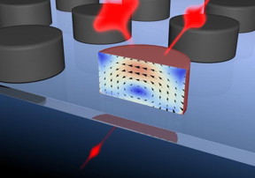 |
| "Device" is a disc 250 nm in diameter that is capable of switching optical pulses at femtosecond rates (femtosecond is a one millionth of one billionth of a second). CREDIT: Maxim Scherbakov et al |
Abstract:
International team of researchers from Lomonosov Moscow State University and the Australian National University in Canberra created an ultrafast all-optical switch on silicon nanostructures. This device may become a platform for future computers and permit to transfer data at an ultrahigh speed. The article with the description of the device was published in Nano Letters journal and highlighted in Nature Materials.
The world's fastest nanoscale photonics switch: Russian scientists developed the world's fastest nanoscale photonics switch
Moscow, Russia | Posted on October 28th, 2015This work belongs to the field of photonics - an optics discipline which appeared in the 1960-s, simultaneously with the invention of lasers. Photonics has the same goals as electronics does, but uses photons--the quanta of light--instead of electrons. The biggest advantage of using photons is the absence of interactions between them. As a consequence, photons address the data transmission problem better than electrons. This property can primarily be used for in computing where IPS (instructions per second) is the main attribute to be maximized. The typical scale of eletronic transistors--the basis of contemporary electronic devices--is less than 100 nanometers, wheres the typical scale of photonic transistors stays on the scale of several micrometers. Nanostructures that are able to compete with the electronic structures--for example, plasmonic nanoparticles--are characterized by low efficiency and significant losses. Therefore, coming up with a compact photonic switch was a very challenging task.
Three years ago several groups of researchers simultaneously discovered an important effect: they found out that silicon nanoparticles are exhibit strong resonances in the visible spectrum - the so-called magnetic dipole resonances. This type of resonance is characterized by strong localization of light waves on subwavelength scales, inside the nanoparticles. This effect turned out to be interesting to researches, but, according to Maxim Shcherbakov, the first author of the article published in Nano Letters, nobody thought that this discovery could create a basis for development of a compact and very rapid photonic switch.
Nanoparticles were fabricated in the Australian National University by e-beam lithography followed by plasma-phase etching. It was done by Alexander Shorokhov, who served an internship in the University as a part of Presidential scholarship for studying abroad. The samples were brought to Moscow, and all the experimental work was carried out at the Faculty of Physics of Lomonosov Moscow State University, in the Laboratory of Nanophotonics and Metamaterials.
"In our experimental research me and my colleague Polina Vabishchevich from the Faculty used a set of nonlinear optics methods that address femtosecond light-matter, -- explains Maxim Shcherbakov. -- We used our femtosecond laser complex acquired as part of the MSU development program".
Eventually, researches developed a "device": a disc 250 nm in diameter that is capable of switching optical pulses at femtosecond rates (femtosecond is a one millionth of one billionth of a second). Switching speeds that fast will allow to create data transmission and processing devices that will work at tens and hundreds terabits per second. This can make possible downloading thousands of HD-movies in less than a second.
The operation of the all-optical switch created by MSU researchers is based on the interaction between two femtosecond pulses. The interaction becomes possible due to the magnetic resonance of the silicon nanostructures. If the pulses arrive at the nanostructure simultaneously, one of them interacts with the other and dampers it due to the effect of two-photon absorption. If there is a 100-fs delay between the two pulses, the interaction does not occur, and the second pulse goes through the nanostructure without changing.
"We were able to develop a structure with the undesirable free-carrier effects are suppressed, -- says Maxim Shcherbakov. -- Free carriers (electrons and electron holes) place serious restrictions on the speed of signal conversion in the traditional integrated photonics. Our work represents an important step towards novel and efficient active photonic devices-- transistors, logic units, and others. Features of the technology implemented in our work will allow its use in silicon photonics. In the nearest future, we are going to test such nanoparticles in integrated circuits".
####
For more information, please click here
Contacts:
Vladimir Koryagin
Copyright © Lomonosov Moscow State University
If you have a comment, please Contact us.Issuers of news releases, not 7th Wave, Inc. or Nanotechnology Now, are solely responsible for the accuracy of the content.
Bookmark:


| Related News Press |
News and information
![]() Quantum computer improves AI predictions April 17th, 2026
Quantum computer improves AI predictions April 17th, 2026
![]() Flexible sensor gains sensitivity under pressure April 17th, 2026
Flexible sensor gains sensitivity under pressure April 17th, 2026
![]() A reusable chip for particulate matter sensing April 17th, 2026
A reusable chip for particulate matter sensing April 17th, 2026
![]() Detecting vibrational quantum beating in the predissociation dynamics of SF6 using time-resolved photoelectron spectroscopy April 17th, 2026
Detecting vibrational quantum beating in the predissociation dynamics of SF6 using time-resolved photoelectron spectroscopy April 17th, 2026
Possible Futures
![]() A fundamentally new therapeutic approach to cystic fibrosis: Nanobody repairs cellular defect April 17th, 2026
A fundamentally new therapeutic approach to cystic fibrosis: Nanobody repairs cellular defect April 17th, 2026
![]() UC Irvine physicists discover method to reverse �quantum scrambling� : The work addresses the problem of information loss in quantum computing system April 17th, 2026
UC Irvine physicists discover method to reverse �quantum scrambling� : The work addresses the problem of information loss in quantum computing system April 17th, 2026
Chip Technology
![]() A reusable chip for particulate matter sensing April 17th, 2026
A reusable chip for particulate matter sensing April 17th, 2026
![]() Metasurfaces smooth light to boost magnetic sensing precision January 30th, 2026
Metasurfaces smooth light to boost magnetic sensing precision January 30th, 2026
Optical computing/Photonic computing
![]() ICFO researchers overcome long-standing bottleneck in single photon detection with twisted 2D materials August 8th, 2025
ICFO researchers overcome long-standing bottleneck in single photon detection with twisted 2D materials August 8th, 2025
![]() Programmable electron-induced color router array May 14th, 2025
Programmable electron-induced color router array May 14th, 2025
Discoveries
![]() Quantum computer improves AI predictions April 17th, 2026
Quantum computer improves AI predictions April 17th, 2026
![]() Flexible sensor gains sensitivity under pressure April 17th, 2026
Flexible sensor gains sensitivity under pressure April 17th, 2026
![]() A reusable chip for particulate matter sensing April 17th, 2026
A reusable chip for particulate matter sensing April 17th, 2026
![]() Detecting vibrational quantum beating in the predissociation dynamics of SF6 using time-resolved photoelectron spectroscopy April 17th, 2026
Detecting vibrational quantum beating in the predissociation dynamics of SF6 using time-resolved photoelectron spectroscopy April 17th, 2026
Materials/Metamaterials/Magnetoresistance
![]() First real-time observation of two-dimensional melting process: Researchers at Mainz University unveil new insights into magnetic vortex structures August 8th, 2025
First real-time observation of two-dimensional melting process: Researchers at Mainz University unveil new insights into magnetic vortex structures August 8th, 2025
![]() Researchers unveil a groundbreaking clay-based solution to capture carbon dioxide and combat climate change June 6th, 2025
Researchers unveil a groundbreaking clay-based solution to capture carbon dioxide and combat climate change June 6th, 2025
![]() A 1960s idea inspires NBI researchers to study hitherto inaccessible quantum states June 6th, 2025
A 1960s idea inspires NBI researchers to study hitherto inaccessible quantum states June 6th, 2025
![]() Institute for Nanoscience hosts annual proposal planning meeting May 16th, 2025
Institute for Nanoscience hosts annual proposal planning meeting May 16th, 2025
Announcements
![]() A fundamentally new therapeutic approach to cystic fibrosis: Nanobody repairs cellular defect April 17th, 2026
A fundamentally new therapeutic approach to cystic fibrosis: Nanobody repairs cellular defect April 17th, 2026
![]() UC Irvine physicists discover method to reverse �quantum scrambling� : The work addresses the problem of information loss in quantum computing system April 17th, 2026
UC Irvine physicists discover method to reverse �quantum scrambling� : The work addresses the problem of information loss in quantum computing system April 17th, 2026
Interviews/Book Reviews/Essays/Reports/Podcasts/Journals/White papers/Posters
![]() A fundamentally new therapeutic approach to cystic fibrosis: Nanobody repairs cellular defect April 17th, 2026
A fundamentally new therapeutic approach to cystic fibrosis: Nanobody repairs cellular defect April 17th, 2026
![]() UC Irvine physicists discover method to reverse �quantum scrambling� : The work addresses the problem of information loss in quantum computing system April 17th, 2026
UC Irvine physicists discover method to reverse �quantum scrambling� : The work addresses the problem of information loss in quantum computing system April 17th, 2026
Photonics/Optics/Lasers
![]() Metasurfaces smooth light to boost magnetic sensing precision January 30th, 2026
Metasurfaces smooth light to boost magnetic sensing precision January 30th, 2026
![]() From sensors to smart systems: the rise of AI-driven photonic noses January 30th, 2026
From sensors to smart systems: the rise of AI-driven photonic noses January 30th, 2026
|
|
||
|
|
||
| The latest news from around the world, FREE | ||
|
|
||
|
|
||
| Premium Products | ||
|
|
||
|
Only the news you want to read!
Learn More |
||
|
|
||
|
Full-service, expert consulting
Learn More |
||
|
|
||