Home > Press > Besi and Imec Present High-Accuracy Narrow-Pitch Bonding of 3D ICs using Thermocompression
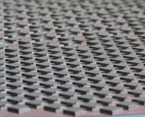 |
| 300 mm wafer with ~900 dies processed on Besi�s new 8800 TC bonder tool. Such an assembly can be finished within 1 hour. |
Abstract:
Today, at SEMICON WEST 2015 (San Francisco), world-leading nano-electronics research center imec and Besi, a global equipment supplier for the semiconductor and electronics industries announced that they have jointly developed an automated thermocompression solution for narrow-pitch die-to-wafer bonding, a method by which singulated dies are stacked onto bottom dies which are still part of a fully intact 300mm wafer. The solution features high accuracy and high throughput, paving the way to a manufacturable 2.5D, 3D, and 2.5D/3D hybrid technology.
Besi and Imec Present High-Accuracy Narrow-Pitch Bonding of 3D ICs using Thermocompression
Leuven, Belgium and Radfeld, Austria | Posted on July 15th, 20153D IC technology, stacking multiple dies into a single device, aims to increase the functionality and performance of next-generation integrated circuits while reducing footprint and power consumption. It is a key technology to enable the next generation of portable electronics, such as smartphones and tablets, which require smaller ICs that consume less power.
One of the challenges to making 3D IC manufacturing an industrial reality is the development of a high-throughput automated process flow for narrow-pitch, high-accuracy die-to-die and die-to-wafer bonding. Thermocompression bonding (TCB) is a widespread process used by the industry for highly accurate die-to-package bonding. The method released the stress in the laminate layer and avoided stress to build up between the two stacked layers. Yet, more traditional approaches to thermocompression bonding come with long cycle times (>1 minute per die), meaning significant improvements in throughput are required to enable this stacking approach on a 300mm wafer.
Imec and Besi have developed an automated TCB process on 300 mm wafers for Besi�s new 8800 TC bonder tool. Imec and Besi demonstrated die-to-wafer bonding at high accuracy, sufficient for 50 �m pitch solder micro bump arrays and a throughput of >1000 UPH with a dual bond head configuration.
�Collaborating with imec, leveraging their expertise on fine pitch bonding materials and processes, has enabled us to develop our 8800 TC bonder tool according to the needs of the semiconductor industry,� said Hugo Pristauz at Besi. �This collaboration has helped us to offer our customers a viable and effective solution for 2.5D/3D IC manufacturing, especially for the new C2W applications.�
####
About IMEC
Imec performs world-leading research in nanoelectronics. Imec leverages its scientific knowledge with the innovative power of its global partnerships in ICT, healthcare and energy. Imec delivers industry-relevant technology solutions. In a unique high-tech environment, its international top talent is committed to providing the building blocks for a better life in a sustainable society. Imec is headquartered in Leuven, Belgium, and has offices in the Netherlands, Taiwan, USA, China, India and Japan. Its staff of about 2,200 people includes almost 700 industrial residents and guest researchers. In 2014, imec's revenue (P&L) totaled 363 million euro. Further information on imec can be found at www.imec.be. Stay up to date about what�s happening at imec with the monthly imec magazine, available for tablets and smartphones (as an app for iOS and Android), or via the website www.imec.be/imecmagazine
Imec is a registered trademark for the activities of IMEC International (a legal entity set up under Belgian law as a "stichting van openbaar nut�), imec Belgium (IMEC vzw supported by the Flemish Government), imec the Netherlands (Stichting IMEC Nederland, part of Holst Centre which is supported by the Dutch Government), imec Taiwan (IMEC Taiwan Co.)and imec China (IMEC Microelectronics (Shanghai) Co. Ltd.) and imec India (Imec India Private Limited).
About Besi
Besi is a leading supplier of semiconductor assembly equipment for the global semiconductor and electronics industries. The Company develops leading edge assembly processes and equipment for leadframe, substrate and wafer level packaging applications in a wide range of end-user markets including electronics, computer, automotive, industrial, RFID, LED and solar energy. Customers are primarily leading semiconductor manufacturers, assembly subcontractors and electronics and industrial companies. Besi�s ordinary shares are listed on NYSE Euronext Amsterdam (symbol: BESI) and OTCQX International (symbol: BESIY) and its headquarters are located in Duiven, the Netherlands. For more information, please visit our website at www.besi.com.
For more information, please click here
Contacts:
Stephanie Black
Business Technology
1215 Cushman Avenue
San Diego, CA 92110
Office 619-234-0345
Copyright © IMEC
If you have a comment, please Contact us.Issuers of news releases, not 7th Wave, Inc. or Nanotechnology Now, are solely responsible for the accuracy of the content.
Bookmark:


| Related News Press |
News and information
![]() Quantum computer improves AI predictions April 17th, 2026
Quantum computer improves AI predictions April 17th, 2026
![]() Flexible sensor gains sensitivity under pressure April 17th, 2026
Flexible sensor gains sensitivity under pressure April 17th, 2026
![]() A reusable chip for particulate matter sensing April 17th, 2026
A reusable chip for particulate matter sensing April 17th, 2026
![]() Detecting vibrational quantum beating in the predissociation dynamics of SF6 using time-resolved photoelectron spectroscopy April 17th, 2026
Detecting vibrational quantum beating in the predissociation dynamics of SF6 using time-resolved photoelectron spectroscopy April 17th, 2026
Chip Technology
![]() A reusable chip for particulate matter sensing April 17th, 2026
A reusable chip for particulate matter sensing April 17th, 2026
![]() Metasurfaces smooth light to boost magnetic sensing precision January 30th, 2026
Metasurfaces smooth light to boost magnetic sensing precision January 30th, 2026
Nanoelectronics
![]() Lab to industry: InSe wafer-scale breakthrough for future electronics August 8th, 2025
Lab to industry: InSe wafer-scale breakthrough for future electronics August 8th, 2025
![]() Interdisciplinary: Rice team tackles the future of semiconductors Multiferroics could be the key to ultralow-energy computing October 6th, 2023
Interdisciplinary: Rice team tackles the future of semiconductors Multiferroics could be the key to ultralow-energy computing October 6th, 2023
![]() Key element for a scalable quantum computer: Physicists from Forschungszentrum J�lich and RWTH Aachen University demonstrate electron transport on a quantum chip September 23rd, 2022
Key element for a scalable quantum computer: Physicists from Forschungszentrum J�lich and RWTH Aachen University demonstrate electron transport on a quantum chip September 23rd, 2022
![]() Reduced power consumption in semiconductor devices September 23rd, 2022
Reduced power consumption in semiconductor devices September 23rd, 2022
Announcements
![]() A fundamentally new therapeutic approach to cystic fibrosis: Nanobody repairs cellular defect April 17th, 2026
A fundamentally new therapeutic approach to cystic fibrosis: Nanobody repairs cellular defect April 17th, 2026
![]() UC Irvine physicists discover method to reverse �quantum scrambling� : The work addresses the problem of information loss in quantum computing system April 17th, 2026
UC Irvine physicists discover method to reverse �quantum scrambling� : The work addresses the problem of information loss in quantum computing system April 17th, 2026
Alliances/Trade associations/Partnerships/Distributorships
![]() Chicago Quantum Exchange welcomes six new partners highlighting quantum technology solutions, from Chicago and beyond September 23rd, 2022
Chicago Quantum Exchange welcomes six new partners highlighting quantum technology solutions, from Chicago and beyond September 23rd, 2022
![]() University of Illinois Chicago joins Brookhaven Lab's Quantum Center June 10th, 2022
University of Illinois Chicago joins Brookhaven Lab's Quantum Center June 10th, 2022
|
|
||
|
|
||
| The latest news from around the world, FREE | ||
|
|
||
|
|
||
| Premium Products | ||
|
|
||
|
Only the news you want to read!
Learn More |
||
|
|
||
|
Full-service, expert consulting
Learn More |
||
|
|
||