Home > Press > Graphene-based film can be used for efficient cooling of electronics
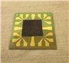 |
| Graphene-based film on an electronic component with high heat intensity. Credit: Johan Liu/Chalmers |
Abstract:
Researchers at Chalmers University of Technology have developed a method for efficiently cooling electronics using graphene-based film. The film has a thermal conductivity capacity that is four times that of copper. Moreover, the graphene film is attachable to electronic components made of silicon, which favours the film’s performance compared to typical graphene characteristics shown in previous, similar experiments.
Graphene-based film can be used for efficient cooling of electronics
Gothenburg, Sweden | Posted on July 10th, 2015Electronic systems available today accumulate a great deal of heat, mostly due to the ever-increasing demand on functionality. Getting rid of excess heat in efficient ways is imperative to prolonging electronic lifespan, and would also lead to a considerable reduction in energy usage. According to an American study, approximately half the energy required to run computer servers, is used for cooling purposes alone.
A couple of years ago, a research team led by Johan Liu, professor at Chalmers University of Technology, were the first to show that graphene can have a cooling effect on silicon-based electronics. That was the starting point for researchers conducting research on the cooling of silicon-based electronics using graphene.
“But the methods that have been in place so far have presented the researchers with problems”, Johan Liu says. “It has become evident that those methods cannot be used to rid electronic devices off great amounts of heat, because they have consisted only of a few layers of thermal conductive atoms. When you try to add more layers of graphene, another problem arises, a problem with adhesiveness. After having increased the amount of layers, the graphene no longer will adhere to the surface, since the adhesion is held together only by weak van der Waals bonds."
“We have now solved this problem by managing to create strong covalent bonds between the graphene film and the surface, which is an electronic component made of silicon,” he continues.
The stronger bonds result from so-called functionalisation of the graphene, i.e. the addition of a property-altering molecule. Having tested several different additives, the Chalmers researchers concluded that an addition of (3-Aminopropyl) triethoxysilane (APTES) molecules has the most desired effect. When heated and put through hydrolysis, it creates so-called silane bonds between the graphene and the electronic component (see picture).
Moreover, functionalisation using silane coupling doubles the thermal conductivity of the graphene. The researchers have shown that the in-plane thermal conductivity of the graphene-based film, with 20 micrometer thickness, can reach a thermal conductivity value of 1600 W/mK, which is four times that of copper.
“Increased thermal capacity could lead to several new applications for graphene,” says Johan Liu. "One example is the integration of graphene-based film into microelectronic devices and systems, such as highly efficient Light Emitting Diodes (LEDs), lasers and radio frequency components for cooling purposes. Graphene-based film could also pave the way for faster, smaller, more energy efficient, sustainable high power electronics."
The research was conducted in collaboration with Shanghai University in China, Ecole Centrale Paris and EM2C – CNRS in France, and SHT Smart High Tech in Sweden.
####
About Chalmers University of Technology
Chalmers University of Technology performs research and education in technology, science and architecture, with a sustainable future as overall vision. Chalmers is well-known for providing an effective environment for innovation and has eight Areas of Advance – Built Environment, Energy, Information and Communication Technology, Life Science, Materials Science, Nanoscience and Nanotechnology, Production, and Transportation. Situated in Gothenburg, Sweden, Chalmers has 13,000 students and 2,500 employees.
For more information, please click here
Contacts:
Johan Liu
professor of Bionano Systems
Chalmers University of Technology
Sweden
+46 31 772 30 67
+46 70 569 38 21,
Christian Borg
+46 - (0)31 772 3395
Copyright © AlphaGalileo Ltd
If you have a comment, please Contact us.Issuers of news releases, not 7th Wave, Inc. or Nanotechnology Now, are solely responsible for the accuracy of the content.
Bookmark:


| Related Links |
![]() Full bibliographic information
Full bibliographic information
| Related News Press |
News and information
![]() Quantum computer improves AI predictions April 17th, 2026
Quantum computer improves AI predictions April 17th, 2026
![]() Flexible sensor gains sensitivity under pressure April 17th, 2026
Flexible sensor gains sensitivity under pressure April 17th, 2026
![]() A reusable chip for particulate matter sensing April 17th, 2026
A reusable chip for particulate matter sensing April 17th, 2026
![]() Detecting vibrational quantum beating in the predissociation dynamics of SF6 using time-resolved photoelectron spectroscopy April 17th, 2026
Detecting vibrational quantum beating in the predissociation dynamics of SF6 using time-resolved photoelectron spectroscopy April 17th, 2026
Thin films
![]() Tiny nanosheets, big leap: A new sensor detects ethanol at ultra-low levels January 30th, 2026
Tiny nanosheets, big leap: A new sensor detects ethanol at ultra-low levels January 30th, 2026
![]() Understanding the mechanism of non-uniform formation of diamond film on tools: Paving the way to a dry process with less environmental impact March 24th, 2023
Understanding the mechanism of non-uniform formation of diamond film on tools: Paving the way to a dry process with less environmental impact March 24th, 2023
![]() New study introduces the best graphite films: The work by Distinguished Professor Feng Ding at UNIST has been published in the October 2022 issue of Nature Nanotechnology November 4th, 2022
New study introduces the best graphite films: The work by Distinguished Professor Feng Ding at UNIST has been published in the October 2022 issue of Nature Nanotechnology November 4th, 2022
![]() Thin-film, high-frequency antenna array offers new flexibility for wireless communications November 5th, 2021
Thin-film, high-frequency antenna array offers new flexibility for wireless communications November 5th, 2021
Display technology/LEDs/SS Lighting/OLEDs
![]() Spinel-type sulfide semiconductors to operate the next-generation LEDs and solar cells For solar-cell absorbers and green-LED source October 3rd, 2025
Spinel-type sulfide semiconductors to operate the next-generation LEDs and solar cells For solar-cell absorbers and green-LED source October 3rd, 2025
Graphene/ Graphite
![]() Electrifying results shed light on graphene foam as a potential material for lab grown cartilage June 6th, 2025
Electrifying results shed light on graphene foam as a potential material for lab grown cartilage June 6th, 2025
![]() Breakthrough in proton barrier films using pore-free graphene oxide: Kumamoto University researchers achieve new milestone in advanced coating technologies September 13th, 2024
Breakthrough in proton barrier films using pore-free graphene oxide: Kumamoto University researchers achieve new milestone in advanced coating technologies September 13th, 2024
Hardware
![]() The present and future of computing get a boost from new research July 21st, 2023
The present and future of computing get a boost from new research July 21st, 2023
Chip Technology
![]() A reusable chip for particulate matter sensing April 17th, 2026
A reusable chip for particulate matter sensing April 17th, 2026
![]() Metasurfaces smooth light to boost magnetic sensing precision January 30th, 2026
Metasurfaces smooth light to boost magnetic sensing precision January 30th, 2026
Discoveries
![]() Quantum computer improves AI predictions April 17th, 2026
Quantum computer improves AI predictions April 17th, 2026
![]() Flexible sensor gains sensitivity under pressure April 17th, 2026
Flexible sensor gains sensitivity under pressure April 17th, 2026
![]() A reusable chip for particulate matter sensing April 17th, 2026
A reusable chip for particulate matter sensing April 17th, 2026
![]() Detecting vibrational quantum beating in the predissociation dynamics of SF6 using time-resolved photoelectron spectroscopy April 17th, 2026
Detecting vibrational quantum beating in the predissociation dynamics of SF6 using time-resolved photoelectron spectroscopy April 17th, 2026
Announcements
![]() A fundamentally new therapeutic approach to cystic fibrosis: Nanobody repairs cellular defect April 17th, 2026
A fundamentally new therapeutic approach to cystic fibrosis: Nanobody repairs cellular defect April 17th, 2026
![]() UC Irvine physicists discover method to reverse ‘quantum scrambling’ : The work addresses the problem of information loss in quantum computing system April 17th, 2026
UC Irvine physicists discover method to reverse ‘quantum scrambling’ : The work addresses the problem of information loss in quantum computing system April 17th, 2026
Interviews/Book Reviews/Essays/Reports/Podcasts/Journals/White papers/Posters
![]() A fundamentally new therapeutic approach to cystic fibrosis: Nanobody repairs cellular defect April 17th, 2026
A fundamentally new therapeutic approach to cystic fibrosis: Nanobody repairs cellular defect April 17th, 2026
![]() UC Irvine physicists discover method to reverse ‘quantum scrambling’ : The work addresses the problem of information loss in quantum computing system April 17th, 2026
UC Irvine physicists discover method to reverse ‘quantum scrambling’ : The work addresses the problem of information loss in quantum computing system April 17th, 2026
Photonics/Optics/Lasers
![]() Metasurfaces smooth light to boost magnetic sensing precision January 30th, 2026
Metasurfaces smooth light to boost magnetic sensing precision January 30th, 2026
![]() From sensors to smart systems: the rise of AI-driven photonic noses January 30th, 2026
From sensors to smart systems: the rise of AI-driven photonic noses January 30th, 2026
Research partnerships
![]() Lab to industry: InSe wafer-scale breakthrough for future electronics August 8th, 2025
Lab to industry: InSe wafer-scale breakthrough for future electronics August 8th, 2025
![]() HKU physicists uncover hidden order in the quantum world through deconfined quantum critical points April 25th, 2025
HKU physicists uncover hidden order in the quantum world through deconfined quantum critical points April 25th, 2025
|
|
||
|
|
||
| The latest news from around the world, FREE | ||
|
|
||
|
|
||
| Premium Products | ||
|
|
||
|
Only the news you want to read!
Learn More |
||
|
|
||
|
Full-service, expert consulting
Learn More |
||
|
|
||