Home > Press > Sweeping lasers snap together nanoscale geometric grids: New technique creates multi-layered, self-assembled grids with fully customizable shapes and compositions
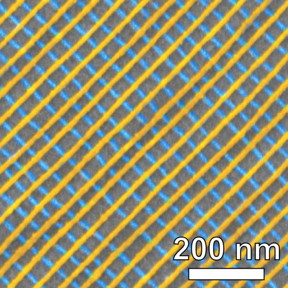 |
| This is a scanning electron microscope image of a self-assembled platinum lattice, false-colored to show the two-layer structure. Each inner square of the nanoscale grid is just 34 nanometers on each side. CREDIT: Brookhaven National Laboratory |
Abstract:
Down at the nanoscale, where objects span just billionths of a meter, the size and shape of a material can often have surprising and powerful electronic and optical effects. Building larger materials that retain subtle nanoscale features is an ongoing challenge that shapes countless emerging technologies.
Sweeping lasers snap together nanoscale geometric grids: New technique creates multi-layered, self-assembled grids with fully customizable shapes and compositions
Upton, NY | Posted on June 23rd, 2015Now, scientists at the U.S. Department of Energy's Brookhaven National Laboratory have developed a new technique to rapidly create nano-structured grids for functional materials with unprecedented versatility.
"We can fabricate multi-layer grids composed of different materials in virtually any geometric configuration," said study coauthor and Brookhaven Lab scientist Kevin Yager. "By quickly and independently controlling the nanoscale structure and the composition, we can tailor the performance of these materials. Crucially, the process can be easily adapted for large-scale applications."
The results--published online June 23 in the journal Nature Communications--could transform the manufacture of high-tech coatings for anti-reflective surfaces, improved solar cells, and touchscreen electronics.
The scientists synthesized the materials at Brookhaven Lab's Center for Functional Nanomaterials (CFN) and characterized the nanoscale architectures using electron microscopy at CFN and x-ray scattering at the National Synchrotron Light Source--both DOE Office of Science User Facilities.
The new technique relies on polymer self-assembly, where molecules are designed to spontaneously assemble into desired structures. Self-assembly requires a burst of heat to make the molecules snap into the proper configurations. Here, an intensely hot laser swept across the sample to transform disordered polymer blocks into precise arrangements in just seconds.
"Self-assembled structures tend to automatically follow molecular preferences, making custom architectures challenging," said lead author Pawel Majewski, a postdoctoral researcher at Brookhaven. "Our laser technique forces the materials to assemble in a particular way. We can then build structures layer-by-layer, constructing lattices composed of squares, rhombuses, triangles, and other shapes."
Laser-assembled nano-wires
For the first step in grid construction, the team took advantage of their recent invention of laser zone annealing (LZA) to produce the extremely localized thermal spikes needed to drive ultra-fast self-assembly.
To further exploit the power and precision of LZA, the researchers applied a heat-sensitive elastic coating on top of the unassembled polymer film. The sweeping laser's heat causes the elastic layer to expand--like shrink-wrap in reverse--which pulls and aligns the rapidly forming nanoscale cylinders.
"The end result is that in less than one second, we can create highly aligned batches of nano-cylinders," said study coauthor Charles Black, who leads the Electronic Nanomaterials group at CFN. "This order persists over macroscopic areas and would be difficult to achieve with any other method."
To make these two-dimensional grids functional, the scientists converted the polymer base into other materials.
One method involved taking the nano-cylinder layer and dipping it into a solution containing metal salts. These molecules then glom onto the self-assembled polymer, converting it into a metallic mesh. A wide range of reactive or conductive metals can be used, including platinum, gold, and palladium.
They also used a technique called vapor deposition, where a vaporized material infiltrates the polymer nano-cylinders and transforms them into functional nano-wires.
Layer-by-layer lattice
The first completed nano-wire array acts as the foundation of the full lattice. Additional layers, each one following variations on that same process, are then stacked to produce customized, crisscrossing configurations--like chain-link fences 10,000 times thinner than a human hair.
"The direction of the laser sweeping across each unassembled layer determines the orientation of the nano-wire rows," Yager said. "We shift that laser direction on each layer, and the way the rows intersect and overlap shapes the grid. We then apply the functional materials after each layer forms. It's an exceptionally fast and simple way to produce such precise configurations."
Study coauthor Atikur Rahman, a CFN postdoctoral researcher, added, "We can stack metals on insulators, too, embedding different functional properties and interactions within one lattice structure.
"The size and the composition of the mesh make a huge difference," Rahman continued. "For example, a single layer of platinum nano-wires conducts electricity in only one direction, but a two-layer mesh conducts uniformly in all directions."
LZA is precise and powerful enough to overcome interface interactions, allowing it to drive polymer self-assembly even on top of complex underlying layers. This versatility enables the use of a wide variety of materials in different nanoscale configurations.
"We can generate nearly any two-dimensional lattice shape, and thus have a lot of freedom in fabricating multi-component nanostructures," Yager said. "It's hard to anticipate all the technologies this rapid and versatile technique will allow."
####
About Brookhaven National Laboratory
Brookhaven National Laboratory is supported by the Office of Science of the U.S. Department of Energy. The Office of Science is the single largest supporter of basic research in the physical sciences in the United States, and is working to address some of the most pressing challenges of our time. For more information, please visit science.energy.gov.
One of ten national laboratories overseen and primarily funded by the Office of Science of the U.S. Department of Energy (DOE), Brookhaven National Laboratory conducts research in the physical, biomedical, and environmental sciences, as well as in energy technologies and national security. Brookhaven Lab also builds and operates major scientific facilities available to university, industry and government researchers. Brookhaven is operated and managed for DOE's Office of Science by Brookhaven Science Associates, a limited-liability company founded by the Research Foundation for the State University of New York on behalf of Stony Brook University, the largest academic user of Laboratory facilities, and Battelle, a nonprofit applied science and technology organization.
For more information, please click here
Contacts:
Justin Eure
631-344-2347
Peter Genzer
631-344-3174
Copyright © Brookhaven National Laboratory
If you have a comment, please Contact us.Issuers of news releases, not 7th Wave, Inc. or Nanotechnology Now, are solely responsible for the accuracy of the content.
Bookmark:


| Related News Press |
News and information
![]() Quantum computer improves AI predictions April 17th, 2026
Quantum computer improves AI predictions April 17th, 2026
![]() Flexible sensor gains sensitivity under pressure April 17th, 2026
Flexible sensor gains sensitivity under pressure April 17th, 2026
![]() A reusable chip for particulate matter sensing April 17th, 2026
A reusable chip for particulate matter sensing April 17th, 2026
![]() Detecting vibrational quantum beating in the predissociation dynamics of SF6 using time-resolved photoelectron spectroscopy April 17th, 2026
Detecting vibrational quantum beating in the predissociation dynamics of SF6 using time-resolved photoelectron spectroscopy April 17th, 2026
Imaging
![]() Simple algorithm paired with standard imaging tool could predict failure in lithium metal batteries August 8th, 2025
Simple algorithm paired with standard imaging tool could predict failure in lithium metal batteries August 8th, 2025
![]() First real-time observation of two-dimensional melting process: Researchers at Mainz University unveil new insights into magnetic vortex structures August 8th, 2025
First real-time observation of two-dimensional melting process: Researchers at Mainz University unveil new insights into magnetic vortex structures August 8th, 2025
![]() New imaging approach transforms study of bacterial biofilms August 8th, 2025
New imaging approach transforms study of bacterial biofilms August 8th, 2025
Laboratories
![]() Researchers develop molecular qubits that communicate at telecom frequencies October 3rd, 2025
Researchers develop molecular qubits that communicate at telecom frequencies October 3rd, 2025
Govt.-Legislation/Regulation/Funding/Policy
![]() Quantum computer improves AI predictions April 17th, 2026
Quantum computer improves AI predictions April 17th, 2026
![]() Metasurfaces smooth light to boost magnetic sensing precision January 30th, 2026
Metasurfaces smooth light to boost magnetic sensing precision January 30th, 2026
![]() New imaging approach transforms study of bacterial biofilms August 8th, 2025
New imaging approach transforms study of bacterial biofilms August 8th, 2025
Self Assembly
![]() Diamond glitter: A play of colors with artificial DNA crystals May 17th, 2024
Diamond glitter: A play of colors with artificial DNA crystals May 17th, 2024
![]() Liquid crystal templated chiral nanomaterials October 14th, 2022
Liquid crystal templated chiral nanomaterials October 14th, 2022
![]() Nanoclusters self-organize into centimeter-scale hierarchical assemblies April 22nd, 2022
Nanoclusters self-organize into centimeter-scale hierarchical assemblies April 22nd, 2022
![]() Atom by atom: building precise smaller nanoparticles with templates March 4th, 2022
Atom by atom: building precise smaller nanoparticles with templates March 4th, 2022
Discoveries
![]() Quantum computer improves AI predictions April 17th, 2026
Quantum computer improves AI predictions April 17th, 2026
![]() Flexible sensor gains sensitivity under pressure April 17th, 2026
Flexible sensor gains sensitivity under pressure April 17th, 2026
![]() A reusable chip for particulate matter sensing April 17th, 2026
A reusable chip for particulate matter sensing April 17th, 2026
![]() Detecting vibrational quantum beating in the predissociation dynamics of SF6 using time-resolved photoelectron spectroscopy April 17th, 2026
Detecting vibrational quantum beating in the predissociation dynamics of SF6 using time-resolved photoelectron spectroscopy April 17th, 2026
Announcements
![]() A fundamentally new therapeutic approach to cystic fibrosis: Nanobody repairs cellular defect April 17th, 2026
A fundamentally new therapeutic approach to cystic fibrosis: Nanobody repairs cellular defect April 17th, 2026
![]() UC Irvine physicists discover method to reverse �quantum scrambling� : The work addresses the problem of information loss in quantum computing system April 17th, 2026
UC Irvine physicists discover method to reverse �quantum scrambling� : The work addresses the problem of information loss in quantum computing system April 17th, 2026
Interviews/Book Reviews/Essays/Reports/Podcasts/Journals/White papers/Posters
![]() A fundamentally new therapeutic approach to cystic fibrosis: Nanobody repairs cellular defect April 17th, 2026
A fundamentally new therapeutic approach to cystic fibrosis: Nanobody repairs cellular defect April 17th, 2026
![]() UC Irvine physicists discover method to reverse �quantum scrambling� : The work addresses the problem of information loss in quantum computing system April 17th, 2026
UC Irvine physicists discover method to reverse �quantum scrambling� : The work addresses the problem of information loss in quantum computing system April 17th, 2026
Industrial
![]() Tiny nanosheets, big leap: A new sensor detects ethanol at ultra-low levels January 30th, 2026
Tiny nanosheets, big leap: A new sensor detects ethanol at ultra-low levels January 30th, 2026
![]() Quantum interference in molecule-surface collisions February 28th, 2025
Quantum interference in molecule-surface collisions February 28th, 2025
![]() Boron nitride nanotube fibers get real: Rice lab creates first heat-tolerant, stable fibers from wet-spinning process June 24th, 2022
Boron nitride nanotube fibers get real: Rice lab creates first heat-tolerant, stable fibers from wet-spinning process June 24th, 2022
Photonics/Optics/Lasers
![]() Metasurfaces smooth light to boost magnetic sensing precision January 30th, 2026
Metasurfaces smooth light to boost magnetic sensing precision January 30th, 2026
![]() From sensors to smart systems: the rise of AI-driven photonic noses January 30th, 2026
From sensors to smart systems: the rise of AI-driven photonic noses January 30th, 2026
|
|
||
|
|
||
| The latest news from around the world, FREE | ||
|
|
||
|
|
||
| Premium Products | ||
|
|
||
|
Only the news you want to read!
Learn More |
||
|
|
||
|
Full-service, expert consulting
Learn More |
||
|
|
||