Home > Press > Moving sector walls on the nano scale
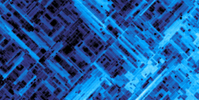 |
| Strontium manganite is a multiferroic, here present in a thin crystal layer. This magnified image shows the individual domains, which are only about 100 nanometres wide. Image: Becher C et al., Nature Nanotechnology 2015 |
Abstract:
Most magnetic materials have a structure that is somewhat more complicated than a commercially available domestic magnet: they not only have a north and south pole, but a variety of sectors, often only a few nanometres in size, in each of which the magnetic axis points in a different direction. These sectors are referred to as domains. Over the past few years, Manfred Fiebig, Professor for Multifunctional Ferroics at ETH Zurich, has been studying the walls between adjoining domains in certain materials. "The inner workings of a material and its domains are one area of interest," says Fiebig. "However, fascinating things also take place at the boundaries of these domains."
Moving sector walls on the nano scale
Zurich, Switzerland | Posted on June 6th, 2015In this work, Fiebig has devoted himself to a very special class of materials: oxides - specifically those with multiferroic properties. These are crystalline materials that are magnetically ordered (i.e. they have a magnetic north and south pole), but at the same time also exhibit an electrical order (that is, the electric charge in the material is distributed so that in addition to the magnetic poles, there are also positive and negative electrical poles).
"That fact that magnetic and electrical ordering occur alongside one another in multiferroic materials means that cross couplings are also possible; for example, the magnetic state can be changed using an electrical voltage," explains Fiebig. These properties make the materials interesting for many applications and are the main reason why they are being researched so intensively by the scientific community.
Tiny capacitors
Together with his fellow researchers, Fiebig has closely studied the domain boundaries in certain multiferroics and recently published two articles on the topic. Here, the scientists showed that the electrical conductivity of the domain walls differs from that of the material as a whole. In one material, strontium manganite, they showed that the domain walls suppress the flow of electric current. "A material with non-conductive walls in a conductive environment could be very useful in the field of electronics," says Fiebig. For example, it may be possible to produce electronic components in which the nanoscale domains act as tiny capacitors that could be electrically charged separately.
"This could be used to create a new charge-based storage medium," says Fiebig. It would take only a voltage pulse to alter the charge in a domain, he adds; a current flow would not be necessary. A storage medium of this type would be more energy-efficient than those available today. In addition, as the data storage would not produce any waste heat that would then need to be dissipated, much smaller storage media could be built.
The paper was co-authored by scientists from Fiebig's research group together with scientists from the group under ETH professor Nicola Spaldin and from the University of Zaragoza. Spaldin and her colleagues contributed the theoretical explanation of why the domain walls are not conductive in strontium manganite. Fiebig explains that as crystalline materials never have a perfect structure, individual oxygen atoms will be missing at certain points in the oxides' crystal lattice. The scientists have now been able to show that these 'oxygen vacancies' accumulate preferentially at the domain boundaries, where they block the flow of current.
Manual change of conductivity
In studies of a second multiferroic material, terbium manganite, scientists from Fiebig's group worked with colleagues from Japan to show that the domain boundaries could also be shifted using electrical fields under certain conditions. "This is an advantage over conventional semiconductor materials, which have a mature, fixed structure," says Fiebig. Furthermore, the researchers found conditions under which it was possible to change the magnetisation of the domains and the conductivity of the domain boundaries without changing the position of the boundaries.
The prerequisite for these studies is a technique that makes the domains and their boundaries visible. This is currently possible only with a specific optical method known as second harmonic generation, where the material is irradiated with a very intense, pulsed laser beam in a specific colour. In response, the material emits light of a different colour, from which the scientists can obtain information on the magnetic and electrical structure of the material. Over the last few years, Fiebig has been the driving force behind the development of this optical method to study the internal order of materials.
New technical possibilities
The fact that it is now possible not only to see the domain walls in a multiferroic, but also to selectively shift them or alter their conductance paves the way for new technical possibilities. Although Fiebig makes clear that specific applications are still a long way off, the findings may in future be used not only in data storage, but also in sensors or complex electronic components. "If you can alter the conductance in a material, you have got a switch - in our case, a switch that you can control without moving anything mechanically and which is therefore not subject to material fatigue," says Fiebig, who is now already thinking about the next step in development. At the moment, the magnetic state can be altered with an electric field. In future, he says, it may be possible to dispense with the electric field and switch the state entirely optically by using the intense light pulses not only to make the internal structure visible but also to simultaneously change it.
####
For more information, please click here
Contacts:
Prof. Manfred Fiebig
41-446-332-690
Copyright © ETH Zurich
If you have a comment, please Contact us.Issuers of news releases, not 7th Wave, Inc. or Nanotechnology Now, are solely responsible for the accuracy of the content.
Bookmark:


| Related Links |
| Related News Press |
News and information
![]() Quantum computer improves AI predictions April 17th, 2026
Quantum computer improves AI predictions April 17th, 2026
![]() Flexible sensor gains sensitivity under pressure April 17th, 2026
Flexible sensor gains sensitivity under pressure April 17th, 2026
![]() A reusable chip for particulate matter sensing April 17th, 2026
A reusable chip for particulate matter sensing April 17th, 2026
![]() Detecting vibrational quantum beating in the predissociation dynamics of SF6 using time-resolved photoelectron spectroscopy April 17th, 2026
Detecting vibrational quantum beating in the predissociation dynamics of SF6 using time-resolved photoelectron spectroscopy April 17th, 2026
Chip Technology
![]() A reusable chip for particulate matter sensing April 17th, 2026
A reusable chip for particulate matter sensing April 17th, 2026
![]() Metasurfaces smooth light to boost magnetic sensing precision January 30th, 2026
Metasurfaces smooth light to boost magnetic sensing precision January 30th, 2026
Memory Technology
![]() Researchers tackle the memory bottleneck stalling quantum computing October 3rd, 2025
Researchers tackle the memory bottleneck stalling quantum computing October 3rd, 2025
![]() First real-time observation of two-dimensional melting process: Researchers at Mainz University unveil new insights into magnetic vortex structures August 8th, 2025
First real-time observation of two-dimensional melting process: Researchers at Mainz University unveil new insights into magnetic vortex structures August 8th, 2025
![]() Utilizing palladium for addressing contact issues of buried oxide thin film transistors April 5th, 2024
Utilizing palladium for addressing contact issues of buried oxide thin film transistors April 5th, 2024
Sensors
![]() Flexible sensor gains sensitivity under pressure April 17th, 2026
Flexible sensor gains sensitivity under pressure April 17th, 2026
![]() Tiny nanosheets, big leap: A new sensor detects ethanol at ultra-low levels January 30th, 2026
Tiny nanosheets, big leap: A new sensor detects ethanol at ultra-low levels January 30th, 2026
![]() From sensors to smart systems: the rise of AI-driven photonic noses January 30th, 2026
From sensors to smart systems: the rise of AI-driven photonic noses January 30th, 2026
![]() Sensors innovations for smart lithium-based batteries: advancements, opportunities, and potential challenges August 8th, 2025
Sensors innovations for smart lithium-based batteries: advancements, opportunities, and potential challenges August 8th, 2025
Discoveries
![]() Quantum computer improves AI predictions April 17th, 2026
Quantum computer improves AI predictions April 17th, 2026
![]() Flexible sensor gains sensitivity under pressure April 17th, 2026
Flexible sensor gains sensitivity under pressure April 17th, 2026
![]() A reusable chip for particulate matter sensing April 17th, 2026
A reusable chip for particulate matter sensing April 17th, 2026
![]() Detecting vibrational quantum beating in the predissociation dynamics of SF6 using time-resolved photoelectron spectroscopy April 17th, 2026
Detecting vibrational quantum beating in the predissociation dynamics of SF6 using time-resolved photoelectron spectroscopy April 17th, 2026
Announcements
![]() A fundamentally new therapeutic approach to cystic fibrosis: Nanobody repairs cellular defect April 17th, 2026
A fundamentally new therapeutic approach to cystic fibrosis: Nanobody repairs cellular defect April 17th, 2026
![]() UC Irvine physicists discover method to reverse �quantum scrambling� : The work addresses the problem of information loss in quantum computing system April 17th, 2026
UC Irvine physicists discover method to reverse �quantum scrambling� : The work addresses the problem of information loss in quantum computing system April 17th, 2026
Interviews/Book Reviews/Essays/Reports/Podcasts/Journals/White papers/Posters
![]() A fundamentally new therapeutic approach to cystic fibrosis: Nanobody repairs cellular defect April 17th, 2026
A fundamentally new therapeutic approach to cystic fibrosis: Nanobody repairs cellular defect April 17th, 2026
![]() UC Irvine physicists discover method to reverse �quantum scrambling� : The work addresses the problem of information loss in quantum computing system April 17th, 2026
UC Irvine physicists discover method to reverse �quantum scrambling� : The work addresses the problem of information loss in quantum computing system April 17th, 2026
|
|
||
|
|
||
| The latest news from around the world, FREE | ||
|
|
||
|
|
||
| Premium Products | ||
|
|
||
|
Only the news you want to read!
Learn More |
||
|
|
||
|
Full-service, expert consulting
Learn More |
||
|
|
||