Home > Press > High-temperature superconductivity in atomically thin films: A route to developing ultimate superconducting nano-devices
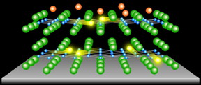 |
| Blue and green circles indicate iron (Fe) and selenium (Se) atoms, respectively. The superconducting transition temperature is tuned by introducing electrons by depositing potassium atoms (orange circles) on the surface. Yellow circles represent a pair of superconducting electrons (Cooper pair). CREDIT: Takashi Takahashi |
Abstract:
A research group at Tohoku University has succeeded in fabricating an atomically thin, high-temperature superconductor film with a superconducting transition temperature (Tc) of up to 60 K (-213°C). The team, led by Prof. Takashi Takahashi (WPI-AIMR) and Asst. Prof. Kosuke Nakayama (Dept. of Physics), also established the method to control/tune the Tc.
High-temperature superconductivity in atomically thin films: A route to developing ultimate superconducting nano-devices
Sendai, Japan | Posted on June 2nd, 2015This finding not only provides an ideal platform for investigating the mechanism of superconductivity in the two-dimensional system, but also paves the way for the development of next-generation nano-scale superconducting devices.
The research results were published in Nature Materials on June 1, 2015.
Superconductors are regarded as one of the most promising candidates for next-generation advanced electronic devices, because the unique quantum effects in superconductors are a great advantage in achieving the energy-saving and ultrahigh-speed processing.
However, the device application of superconductors has long been hindered. The largest obstacle is the necessity of a huge and expensive cooling system with liquid helium, because of the low Tc of conventional superconductors, which is close to absolute zero (0 K, - 273 °C)*1. It has also been a big challenge to realize the high-density integration of superconductors into electronic devices. In order to overcome these problems, it is definitely necessary to develop a new superconductor with higher- Tc, that can be fabricated into a thin film.
The research team at Tohoku University turned its attention to iron selenide (FeSe), which is a member of iron-based superconductors*2. While the Tc of bulk FeSe is only 8 K (-265 °C), a signature of higher-Tc superconductivity has been suggested in ultrathin film and its verification has been urgently required.
The researchers at first fabricated high-quality, atomically thin FeSe films [Fig. 1], with thickness of between one monolayer (which corresponds to three-atoms thickness) and twenty monolayers (sixty-atoms thickness), by using the molecular-beam-epitaxy (MBE) method*3. Then they carefully investigated the electronic structure of grown films by angle-resolved photoemission spectroscopy (ARPES)*4 [Fig. 2].
In the ARPES measurement, the researchers observed the opening of a superconducting gap at low temperature*5, which is direct evidence of the emergence of superconductivity in the films. The researchers found that the Tc estimated from the gap-closing in a monolayer film is surprisingly high (above 60 K), which is about 8 times higher than the Tc of bulk FeSe.
While multilayer films do not show superconductivity in the as-grown state, the researchers have discovered a novel method to deposit alkali atoms onto the films and thereby control the electron density in the film. By employing this method, the researchers have succeeded in converting non-superconducting multilayer FeSe films into high-Tc superconductors with Tc as high as ~50 K.
The present result gives a great impact to both the basic and applied researches in superconductors. The researchers have clearly shown how the superconductivity is emerged, enhanced and controlled in atomically thin FeSe films. While the Tc achieved in this study (50-60 K) is still lower than that of the cuprate high-Tc superconductors (highest Tc?135 K) which caused the "high-Tc fever" in the world 30 years ago, it obviously exceeds the record of other "high-Tc superconductors" such as fullerene (C60) superconductors (Tc~33 K) and MgB2 (Tc~39K), closely approaching the temperature of liquid nitrogen (77 K).
The present report would lead to intensive researches to further increase Tc by changing the number of atomic layers, the amount of doped electrons and the species of substrate. The present result would also widen the range of both basic and applied researches on superconductivity, because the Tc of 50-60 K achieved in the present study is high enough to keep the superconducting state by using a closed-cycle-gas-type cooling system without liquid helium.
The present success in fabricating an atomically thin high-temperature superconductor not only provides an ideal platform to investigate the novel two-dimensional superconductivity, but also opens a route to developing an ultimate superconducting nano-device consisting of atomic-size electronic parts. The ultrathin high-Tc superconductor would effectively contribute to the significant down-sizing and consequent high-density integration in electric circuits, leading to the realization of future-generation electronic devices with high energy-saving and ultrahigh-speed operation.
This work was supported by grants from the Japan Society for the Promotion of Science (JSPS) and Japan's Ministry of Education, Culture, Sports, Science and Technology (MEXT).
###
Manuscript information:
Research team: Y. Miyata, K. Nakayama, K. Sugawara, T. Sato and T. Takahashi
Title: "High-temperature Superconductivity in Potassium-coated Multilayer FeSe Thin Films"
Publication: Nature Materials
Publication Date: June 1, 2015
Terms
*1) K (Kelvin)
A unit of temperature based on the absolute scale. The following relation converts this scale to the scale of degree Celsius (°C). °C = K - 273.15
*2) Iron-based superconductors
A group of superconductors consisting of two-dimensional iron layer, which was first discovered in 2008 by Prof. Hideo Hosono at Tokyo Institute of Technology, Japan.
*3) Molecular-beam-epitaxy method
A method of growing a thin, singlecrystal film on a substrate. Constituent atoms are selectively evaporated and deposited on a substrate under vacuum in a well-controlled manner. This method has an advantage in growing a high-quality single crystal film.
*4) Angle-resolved photoemission spectroscopy
An experimental technique to directly determine the energy and momentum of electrons in solids. It is based on the external photoelectric effect predicted by Einstein. Recent significant improvement of the energy resolution enables the precise investigation of superconducting electrons.
*5) Superconducting gap
An energy cost to create a superconducting electron pair (Cooper pair). The magnitude is directly observed by angle-resolved photoemission spectroscopy.
####
For more information, please click here
Contacts:
Takashi Takahashi
WPI Research Center,
Advanced Institute for Materials Research (WPI-AIMR), Tohoku University
Tel: +81-22-795-6417
Kosuke Nakayama
Department of Physics, Tohoku University
Tel: +81-22-795-6477
For enquiries about WPI-AIMR:
Tel: +81-22-217-6146
Copyright © Tohoku University
If you have a comment, please Contact us.Issuers of news releases, not 7th Wave, Inc. or Nanotechnology Now, are solely responsible for the accuracy of the content.
Bookmark:


| Related News Press |
News and information
![]() Quantum computer improves AI predictions April 17th, 2026
Quantum computer improves AI predictions April 17th, 2026
![]() Flexible sensor gains sensitivity under pressure April 17th, 2026
Flexible sensor gains sensitivity under pressure April 17th, 2026
![]() A reusable chip for particulate matter sensing April 17th, 2026
A reusable chip for particulate matter sensing April 17th, 2026
![]() Detecting vibrational quantum beating in the predissociation dynamics of SF6 using time-resolved photoelectron spectroscopy April 17th, 2026
Detecting vibrational quantum beating in the predissociation dynamics of SF6 using time-resolved photoelectron spectroscopy April 17th, 2026
Superconductivity
![]() MXene nanomaterials enter a new dimension Multilayer nanomaterial: MXene flakes created at Drexel University show new promise as 1D scrolls January 30th, 2026
MXene nanomaterials enter a new dimension Multilayer nanomaterial: MXene flakes created at Drexel University show new promise as 1D scrolls January 30th, 2026
Thin films
![]() Tiny nanosheets, big leap: A new sensor detects ethanol at ultra-low levels January 30th, 2026
Tiny nanosheets, big leap: A new sensor detects ethanol at ultra-low levels January 30th, 2026
Govt.-Legislation/Regulation/Funding/Policy
![]() Quantum computer improves AI predictions April 17th, 2026
Quantum computer improves AI predictions April 17th, 2026
![]() Metasurfaces smooth light to boost magnetic sensing precision January 30th, 2026
Metasurfaces smooth light to boost magnetic sensing precision January 30th, 2026
![]() New imaging approach transforms study of bacterial biofilms August 8th, 2025
New imaging approach transforms study of bacterial biofilms August 8th, 2025
Chip Technology
![]() A reusable chip for particulate matter sensing April 17th, 2026
A reusable chip for particulate matter sensing April 17th, 2026
![]() Metasurfaces smooth light to boost magnetic sensing precision January 30th, 2026
Metasurfaces smooth light to boost magnetic sensing precision January 30th, 2026
Discoveries
![]() Quantum computer improves AI predictions April 17th, 2026
Quantum computer improves AI predictions April 17th, 2026
![]() Flexible sensor gains sensitivity under pressure April 17th, 2026
Flexible sensor gains sensitivity under pressure April 17th, 2026
![]() A reusable chip for particulate matter sensing April 17th, 2026
A reusable chip for particulate matter sensing April 17th, 2026
![]() Detecting vibrational quantum beating in the predissociation dynamics of SF6 using time-resolved photoelectron spectroscopy April 17th, 2026
Detecting vibrational quantum beating in the predissociation dynamics of SF6 using time-resolved photoelectron spectroscopy April 17th, 2026
Announcements
![]() A fundamentally new therapeutic approach to cystic fibrosis: Nanobody repairs cellular defect April 17th, 2026
A fundamentally new therapeutic approach to cystic fibrosis: Nanobody repairs cellular defect April 17th, 2026
![]() UC Irvine physicists discover method to reverse ‘quantum scrambling’ : The work addresses the problem of information loss in quantum computing system April 17th, 2026
UC Irvine physicists discover method to reverse ‘quantum scrambling’ : The work addresses the problem of information loss in quantum computing system April 17th, 2026
Interviews/Book Reviews/Essays/Reports/Podcasts/Journals/White papers/Posters
![]() A fundamentally new therapeutic approach to cystic fibrosis: Nanobody repairs cellular defect April 17th, 2026
A fundamentally new therapeutic approach to cystic fibrosis: Nanobody repairs cellular defect April 17th, 2026
![]() UC Irvine physicists discover method to reverse ‘quantum scrambling’ : The work addresses the problem of information loss in quantum computing system April 17th, 2026
UC Irvine physicists discover method to reverse ‘quantum scrambling’ : The work addresses the problem of information loss in quantum computing system April 17th, 2026
|
|
||
|
|
||
| The latest news from around the world, FREE | ||
|
|
||
|
|
||
| Premium Products | ||
|
|
||
|
Only the news you want to read!
Learn More |
||
|
|
||
|
Full-service, expert consulting
Learn More |
||
|
|
||