Home > Press > Taking control of light emission: Researchers find a way of tuning light waves by pairing 2 exotic 2-D materials
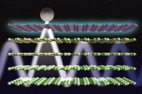 |
| Researchers have shown that a DC voltage applied to layers of graphene and boron nitride can be used to control light emission from a nearby atom. Here, graphene is represented by a maroon-colored top layer; boron nitride is represented by yellow-green lattices below the graphene; and the atom is represented by a grey circle. A low concentration of DC voltage (in blue) allows the light to propagate inside the boron nitride, forming a tightly confined waveguide for optical signals.
Image: Anshuman Kumar Srivastava and Jose Luis Olivares/MIT |
Abstract:
Researchers have found a way to couple the properties of different two-dimensional materials to provide an exceptional degree of control over light waves. They say this has the potential to lead to new kinds of light detection, thermal-management systems, and high-resolution imaging devices.
Taking control of light emission: Researchers find a way of tuning light waves by pairing 2 exotic 2-D materials
Cambridge, MA | Posted on May 20th, 2015The new findings -- using a layer of one-atom-thick graphene deposited on top of a similar 2-D layer of a material called hexagonal boron nitride (hBN) -- are published in the journal Nano Letters. The work is co-authored by MIT associate professor of mechanical engineering Nicholas Fang and graduate student Anshuman Kumar, and their co-authors at IBM's T.J. Watson Research Center, Hong Kong Polytechnic University, and the University of Minnesota.
Although the two materials are structurally similar -- both composed of hexagonal arrays of atoms that form two-dimensional sheets -- they each interact with light quite differently. But the researchers found that these interactions can be complementary, and can couple in ways that afford a great deal of control over the behavior of light.
The hybrid material blocks light when a particular voltage is applied to the graphene, while allowing a special kind of emission and propagation, called "hyperbolicity," when a different voltage is applied -- a phenomenon not seen before in optical systems, Fang says. One of the consequences of this unusual behavior is that an extremely thin sheet of material can interact strongly with light, allowing beams to be guided, funneled, and controlled by voltages applied to the sheet.
"This poses a new opportunity to send and receive light over a very confined space," Fang says, and could lead to "unique optical material that has great potential for optical interconnects." Many researchers see improved interconnection of optical and electronic components as a path to more efficient computation and imaging systems.
Light's interaction with graphene produces particles called plasmons, while light interacting with hBN produces phonons. Fang and his colleagues found that when the materials are combined in a certain way, the plasmons and phonons can couple, producing a strong resonance.
The properties of the graphene allow precise control over light, while hBN provides very strong confinement and guidance of the light. Combining the two makes it possible to create new "metamaterials" that marry the advantages of both, the researchers say.
Phaedon Avouris, a researcher at IBM and co-author of the paper, says, "The combination of these two materials provides a unique system that allows the manipulation of optical processes."
The combined materials create a tuned system that can be adjusted to allow light only of certain specific wavelengths or directions to propagate, they say. "We can start to selectively pick some frequencies [to let through], and reject some," Kumar says.
These properties should make it possible, Fang says, to create tiny optical waveguides, about 20 nanometers in size -- the same size range as the smallest features that can now be produced in microchips. This could lead to chips that combine optical and electronic components in a single device, with far lower losses than when such devices are made separately and then interconnected, they say.
Co-author Tony Low, a researcher at IBM and the University of Minnesota, says, "Our work paves the way for using 2-D material heterostructures for engineering new optical properties on demand."
Another potential application, Fang says, comes from the ability to switch a light beam on and off at the material's surface; because the material naturally works at near-infrared wavelengths, this could enable new avenues for infrared spectroscopy, he says. "It could even enable single-molecule resolution," Fang says, of biomolecules placed on the hybrid material's surface.
###
The research team also included Kin Hung Fung of Hong Kong Polytechnic University. The work was supported by the National Science Foundation and the Air Force Office of Scientific Research.
####
For more information, please click here
Contacts:
Andrew Carleen
617-253-1682
Copyright © Massachusetts Institute of Technology
If you have a comment, please Contact us.Issuers of news releases, not 7th Wave, Inc. or Nanotechnology Now, are solely responsible for the accuracy of the content.
Bookmark:


| Related Links |
![]() Paper: �Tunable light�matter interaction and the role of hyperbolicity in graphene�hBN system�:
Paper: �Tunable light�matter interaction and the role of hyperbolicity in graphene�hBN system�:
| Related News Press |
News and information
![]() Quantum computer improves AI predictions April 17th, 2026
Quantum computer improves AI predictions April 17th, 2026
![]() Flexible sensor gains sensitivity under pressure April 17th, 2026
Flexible sensor gains sensitivity under pressure April 17th, 2026
![]() A reusable chip for particulate matter sensing April 17th, 2026
A reusable chip for particulate matter sensing April 17th, 2026
![]() Detecting vibrational quantum beating in the predissociation dynamics of SF6 using time-resolved photoelectron spectroscopy April 17th, 2026
Detecting vibrational quantum beating in the predissociation dynamics of SF6 using time-resolved photoelectron spectroscopy April 17th, 2026
Imaging
![]() Simple algorithm paired with standard imaging tool could predict failure in lithium metal batteries August 8th, 2025
Simple algorithm paired with standard imaging tool could predict failure in lithium metal batteries August 8th, 2025
Graphene/ Graphite
![]() Electrifying results shed light on graphene foam as a potential material for lab grown cartilage June 6th, 2025
Electrifying results shed light on graphene foam as a potential material for lab grown cartilage June 6th, 2025
![]() Breakthrough in proton barrier films using pore-free graphene oxide: Kumamoto University researchers achieve new milestone in advanced coating technologies September 13th, 2024
Breakthrough in proton barrier films using pore-free graphene oxide: Kumamoto University researchers achieve new milestone in advanced coating technologies September 13th, 2024
Govt.-Legislation/Regulation/Funding/Policy
![]() Quantum computer improves AI predictions April 17th, 2026
Quantum computer improves AI predictions April 17th, 2026
![]() Metasurfaces smooth light to boost magnetic sensing precision January 30th, 2026
Metasurfaces smooth light to boost magnetic sensing precision January 30th, 2026
![]() New imaging approach transforms study of bacterial biofilms August 8th, 2025
New imaging approach transforms study of bacterial biofilms August 8th, 2025
Discoveries
![]() Quantum computer improves AI predictions April 17th, 2026
Quantum computer improves AI predictions April 17th, 2026
![]() Flexible sensor gains sensitivity under pressure April 17th, 2026
Flexible sensor gains sensitivity under pressure April 17th, 2026
![]() A reusable chip for particulate matter sensing April 17th, 2026
A reusable chip for particulate matter sensing April 17th, 2026
![]() Detecting vibrational quantum beating in the predissociation dynamics of SF6 using time-resolved photoelectron spectroscopy April 17th, 2026
Detecting vibrational quantum beating in the predissociation dynamics of SF6 using time-resolved photoelectron spectroscopy April 17th, 2026
Materials/Metamaterials/Magnetoresistance
![]() First real-time observation of two-dimensional melting process: Researchers at Mainz University unveil new insights into magnetic vortex structures August 8th, 2025
First real-time observation of two-dimensional melting process: Researchers at Mainz University unveil new insights into magnetic vortex structures August 8th, 2025
![]() Researchers unveil a groundbreaking clay-based solution to capture carbon dioxide and combat climate change June 6th, 2025
Researchers unveil a groundbreaking clay-based solution to capture carbon dioxide and combat climate change June 6th, 2025
![]() A 1960s idea inspires NBI researchers to study hitherto inaccessible quantum states June 6th, 2025
A 1960s idea inspires NBI researchers to study hitherto inaccessible quantum states June 6th, 2025
![]() Institute for Nanoscience hosts annual proposal planning meeting May 16th, 2025
Institute for Nanoscience hosts annual proposal planning meeting May 16th, 2025
Announcements
![]() A fundamentally new therapeutic approach to cystic fibrosis: Nanobody repairs cellular defect April 17th, 2026
A fundamentally new therapeutic approach to cystic fibrosis: Nanobody repairs cellular defect April 17th, 2026
![]() UC Irvine physicists discover method to reverse �quantum scrambling� : The work addresses the problem of information loss in quantum computing system April 17th, 2026
UC Irvine physicists discover method to reverse �quantum scrambling� : The work addresses the problem of information loss in quantum computing system April 17th, 2026
Interviews/Book Reviews/Essays/Reports/Podcasts/Journals/White papers/Posters
![]() A fundamentally new therapeutic approach to cystic fibrosis: Nanobody repairs cellular defect April 17th, 2026
A fundamentally new therapeutic approach to cystic fibrosis: Nanobody repairs cellular defect April 17th, 2026
![]() UC Irvine physicists discover method to reverse �quantum scrambling� : The work addresses the problem of information loss in quantum computing system April 17th, 2026
UC Irvine physicists discover method to reverse �quantum scrambling� : The work addresses the problem of information loss in quantum computing system April 17th, 2026
Tools
![]() Metasurfaces smooth light to boost magnetic sensing precision January 30th, 2026
Metasurfaces smooth light to boost magnetic sensing precision January 30th, 2026
![]() From sensors to smart systems: the rise of AI-driven photonic noses January 30th, 2026
From sensors to smart systems: the rise of AI-driven photonic noses January 30th, 2026
![]() Japan launches fully domestically produced quantum computer: Expo visitors to experience quantum computing firsthand August 8th, 2025
Japan launches fully domestically produced quantum computer: Expo visitors to experience quantum computing firsthand August 8th, 2025
Military
![]() Quantum engineers �squeeze� laser frequency combs to make more sensitive gas sensors January 17th, 2025
Quantum engineers �squeeze� laser frequency combs to make more sensitive gas sensors January 17th, 2025
![]() Chainmail-like material could be the future of armor: First 2D mechanically interlocked polymer exhibits exceptional flexibility and strength January 17th, 2025
Chainmail-like material could be the future of armor: First 2D mechanically interlocked polymer exhibits exceptional flexibility and strength January 17th, 2025
![]() Single atoms show their true color July 5th, 2024
Single atoms show their true color July 5th, 2024
![]() NRL charters Navy�s quantum inertial navigation path to reduce drift April 5th, 2024
NRL charters Navy�s quantum inertial navigation path to reduce drift April 5th, 2024
Photonics/Optics/Lasers
![]() Metasurfaces smooth light to boost magnetic sensing precision January 30th, 2026
Metasurfaces smooth light to boost magnetic sensing precision January 30th, 2026
![]() From sensors to smart systems: the rise of AI-driven photonic noses January 30th, 2026
From sensors to smart systems: the rise of AI-driven photonic noses January 30th, 2026
Research partnerships
![]() Lab to industry: InSe wafer-scale breakthrough for future electronics August 8th, 2025
Lab to industry: InSe wafer-scale breakthrough for future electronics August 8th, 2025
![]() HKU physicists uncover hidden order in the quantum world through deconfined quantum critical points April 25th, 2025
HKU physicists uncover hidden order in the quantum world through deconfined quantum critical points April 25th, 2025
|
|
||
|
|
||
| The latest news from around the world, FREE | ||
|
|
||
|
|
||
| Premium Products | ||
|
|
||
|
Only the news you want to read!
Learn More |
||
|
|
||
|
Full-service, expert consulting
Learn More |
||
|
|
||