Home > Press > Rutgers, NIST physicists report technology with potential for sub-micron optical switches
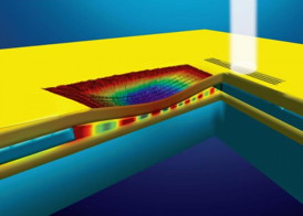 |
| Surface plasmons are propagating electronic oscillations localized to metal-insulator (e.g. gold-air) interfaces. Gap plasmons (GPs) arise when two such interfaces are separated by a narrow gap across the insulator layer, transversely confining the electromagnetic energy in an MIM (metal-insulator-metal) waveguide. In this illustration, a free-space excitation laser (vertical light on the right) couples to GPs (alternating red/blue light) in a gold/air/gold nanofabricated waveguide. A grating is used to match the laser light momentum with to a GP. The GP propagates through the waveguide under free-floating micro-beams in the top gold layer (color coded to show depth). When the beams are electrically actuated towards the bottom gold layer, the effective refractive index of the waveguide increases under the beams, phase-retarding the GP. CREDIT: Brian Dennis, Rutgers University |
Abstract:
A team that includes Rutgers University and National Institute of Standards and Technology scientists believes that a technology it is reporting this week in Nature Photonics could result in optical switches with sub-square-micron footprints, potentially allowing densely packed switching fabrics on a chip.
Rutgers, NIST physicists report technology with potential for sub-micron optical switches
New Brunswick, NJ | Posted on March 31st, 2015These dimensions contrast with established optical switching technologies based on other technologies, such as MEMS, lithium niobate, and silicon and electro-optic polymer plasmonic technologies, that have active elements in scales up to hundreds of microns.
The scientists have shown that an optical signal can be modulated in a 200 nanometer-high waveguide. The signal's phase is modulated as it passes through an air gap between two gold layers, when a force generated by the device slightly deforms the top gold layer.
The scientists propose that when one of these modulators is placed next to a similar static device, it could act as a 2x2 switch, based on evidence reported elsewhere of coupling between adjacent waveguides. The technology could also be useful for electrically tunable plasmonic devices.
Their paper describes "compact nanomechanical plasmonic phase modulators." The scientists experimentally verified such devices in a 23 micron-long waveguide with a gap in the range of 200 nm, but they make a case based on computer modeling that the waveguides can be scaled to as little as 1 micron long with a 20 nm gap, without significant loss. This means optical switches could be scaled closer to electronic device dimensions.
###
The paper's authors are Brian Dennis, Michael Haftel, David Czaplewski, Daniel Lopez, Girsh Blumberg and Vladimir Aksyuk. Funding for this research was provided primarily by the National Institute of Standards and Technology and by the Air Force Office of Scientific Research. The work was performed at the NIST Center for Nanoscale Science and Technology - a national nanotechnology user facility.
####
For more information, please click here
Contacts:
Carl Blesch
848-932-0550
@RutgersU
http://www.rutgers.edu
Mark Esser
301-975-8735
NIST
Copyright © Rutgers University
If you have a comment, please Contact us.Issuers of news releases, not 7th Wave, Inc. or Nanotechnology Now, are solely responsible for the accuracy of the content.
Bookmark:


| Related News Press |
News and information
![]() Quantum computer improves AI predictions April 17th, 2026
Quantum computer improves AI predictions April 17th, 2026
![]() Flexible sensor gains sensitivity under pressure April 17th, 2026
Flexible sensor gains sensitivity under pressure April 17th, 2026
![]() A reusable chip for particulate matter sensing April 17th, 2026
A reusable chip for particulate matter sensing April 17th, 2026
![]() Detecting vibrational quantum beating in the predissociation dynamics of SF6 using time-resolved photoelectron spectroscopy April 17th, 2026
Detecting vibrational quantum beating in the predissociation dynamics of SF6 using time-resolved photoelectron spectroscopy April 17th, 2026
Laboratories
![]() Researchers develop molecular qubits that communicate at telecom frequencies October 3rd, 2025
Researchers develop molecular qubits that communicate at telecom frequencies October 3rd, 2025
![]() A battery�s hopping ions remember where they�ve been: Seen in atomic detail, the seemingly smooth flow of ions through a battery�s electrolyte is surprisingly complicated February 16th, 2024
A battery�s hopping ions remember where they�ve been: Seen in atomic detail, the seemingly smooth flow of ions through a battery�s electrolyte is surprisingly complicated February 16th, 2024
Govt.-Legislation/Regulation/Funding/Policy
![]() Quantum computer improves AI predictions April 17th, 2026
Quantum computer improves AI predictions April 17th, 2026
![]() Metasurfaces smooth light to boost magnetic sensing precision January 30th, 2026
Metasurfaces smooth light to boost magnetic sensing precision January 30th, 2026
![]() New imaging approach transforms study of bacterial biofilms August 8th, 2025
New imaging approach transforms study of bacterial biofilms August 8th, 2025
Chip Technology
![]() A reusable chip for particulate matter sensing April 17th, 2026
A reusable chip for particulate matter sensing April 17th, 2026
![]() Metasurfaces smooth light to boost magnetic sensing precision January 30th, 2026
Metasurfaces smooth light to boost magnetic sensing precision January 30th, 2026
Optical computing/Photonic computing
![]() ICFO researchers overcome long-standing bottleneck in single photon detection with twisted 2D materials August 8th, 2025
ICFO researchers overcome long-standing bottleneck in single photon detection with twisted 2D materials August 8th, 2025
![]() Programmable electron-induced color router array May 14th, 2025
Programmable electron-induced color router array May 14th, 2025
Nanoelectronics
![]() Lab to industry: InSe wafer-scale breakthrough for future electronics August 8th, 2025
Lab to industry: InSe wafer-scale breakthrough for future electronics August 8th, 2025
![]() Interdisciplinary: Rice team tackles the future of semiconductors Multiferroics could be the key to ultralow-energy computing October 6th, 2023
Interdisciplinary: Rice team tackles the future of semiconductors Multiferroics could be the key to ultralow-energy computing October 6th, 2023
![]() Key element for a scalable quantum computer: Physicists from Forschungszentrum J�lich and RWTH Aachen University demonstrate electron transport on a quantum chip September 23rd, 2022
Key element for a scalable quantum computer: Physicists from Forschungszentrum J�lich and RWTH Aachen University demonstrate electron transport on a quantum chip September 23rd, 2022
![]() Reduced power consumption in semiconductor devices September 23rd, 2022
Reduced power consumption in semiconductor devices September 23rd, 2022
Discoveries
![]() Quantum computer improves AI predictions April 17th, 2026
Quantum computer improves AI predictions April 17th, 2026
![]() Flexible sensor gains sensitivity under pressure April 17th, 2026
Flexible sensor gains sensitivity under pressure April 17th, 2026
![]() A reusable chip for particulate matter sensing April 17th, 2026
A reusable chip for particulate matter sensing April 17th, 2026
![]() Detecting vibrational quantum beating in the predissociation dynamics of SF6 using time-resolved photoelectron spectroscopy April 17th, 2026
Detecting vibrational quantum beating in the predissociation dynamics of SF6 using time-resolved photoelectron spectroscopy April 17th, 2026
Announcements
![]() A fundamentally new therapeutic approach to cystic fibrosis: Nanobody repairs cellular defect April 17th, 2026
A fundamentally new therapeutic approach to cystic fibrosis: Nanobody repairs cellular defect April 17th, 2026
![]() UC Irvine physicists discover method to reverse �quantum scrambling� : The work addresses the problem of information loss in quantum computing system April 17th, 2026
UC Irvine physicists discover method to reverse �quantum scrambling� : The work addresses the problem of information loss in quantum computing system April 17th, 2026
Photonics/Optics/Lasers
![]() Metasurfaces smooth light to boost magnetic sensing precision January 30th, 2026
Metasurfaces smooth light to boost magnetic sensing precision January 30th, 2026
![]() From sensors to smart systems: the rise of AI-driven photonic noses January 30th, 2026
From sensors to smart systems: the rise of AI-driven photonic noses January 30th, 2026
Research partnerships
![]() Lab to industry: InSe wafer-scale breakthrough for future electronics August 8th, 2025
Lab to industry: InSe wafer-scale breakthrough for future electronics August 8th, 2025
![]() HKU physicists uncover hidden order in the quantum world through deconfined quantum critical points April 25th, 2025
HKU physicists uncover hidden order in the quantum world through deconfined quantum critical points April 25th, 2025
|
|
||
|
|
||
| The latest news from around the world, FREE | ||
|
|
||
|
|
||
| Premium Products | ||
|
|
||
|
Only the news you want to read!
Learn More |
||
|
|
||
|
Full-service, expert consulting
Learn More |
||
|
|
||