Home > Press > Stacking two-dimensional materials may lower cost of semiconductor devices
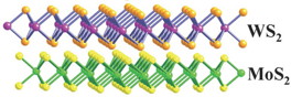 |
| Schematic illustration of monolayer MoS2 and WS2 stacked vertically. Image: Linyou Cao. |
Abstract:
"Equally Efficient Interlayer Exciton Relaxation and Improved Absorption in Epitaxial and Non-epitaxial MoS2/WS2 Heterostructures"
Authors: Yifei Yu, Shi Hu, Lujun Huang, Yi Liu, Zhenghe Jin, Ki Wook Kim, and Linyou Cao, North Carolina State University; Liqin Su and Yong Zhang, University of North Carolina at Charlotte; Alexander A. Purezky and David B. Geohegan, Oak Ridge National Laboratory
Published: Dec. 3, Nano Letters
DOI: 10.1021/nl5038177
Abstract: Semiconductor heterostructures provide a powerful platform to engineer the dynamics of excitons for fundamental and applied interests. However, the functionality of conventional semiconductor heterostructures is often limited by inefficient charge transfer across interfaces due to the interfacial imperfection caused by lattice mismatch. Here we demonstrate that MoS2/WS2 heterostructures consisting of monolayer MoS2 and WS2 stacked in the vertical direction can enable equally efficient interlayer exciton relaxation regardless the epitaxy and orientation of the stacking. This is manifested by a similar two orders of magnitude decrease of photoluminescence intensity in both epitaxial and non-epitaxial MoS2/WS2 heterostructures. Both heterostructures also show similarly improved absorption beyond the simple super-imposition of the absorptions of monolayer MoS2 and WS2. Our result indicates that 2D heterostructures bear significant implications for the development of photonic devices, in particular those requesting efficient exciton separation and strong light absorption, such as solar cells, photodetectors, modulators, and photocatalysts. It also suggests that the simple stacking of dissimilar 2D materials with random orientations is a viable strategy to fabricate complex functional 2D heterostructures, which would show similar optical functionality as the counterpart with perfect epitaxy.
Stacking two-dimensional materials may lower cost of semiconductor devices
Raleigh, NC | Posted on December 11th, 2014A team of researchers led by North Carolina State University has found that stacking materials that are only one atom thick can create semiconductor junctions that transfer charge efficiently, regardless of whether the crystalline structure of the materials is mismatched - lowering the manufacturing cost for a wide variety of semiconductor devices such as solar cells, lasers and LEDs.
"This work demonstrates that by stacking multiple two-dimensional (2-D) materials in random ways we can create semiconductor junctions that are as functional as those with perfect alignment" says Dr. Linyou Cao, senior author of a paper on the work and an assistant professor of materials science and engineering at NC State.
"This could make the manufacture of semiconductor devices an order of magnitude less expensive."
For most semiconductor electronic or photonic devices to work, they need to have a junction, which is where two semiconductor materials are bound together. For example, in photonic devices like solar cells, lasers and LEDs, the junction is where photons are converted into electrons, or vice versa.
All semiconductor junctions rely on efficient charge transfer between materials, to ensure that current flows smoothly and that a minimum of energy is lost during the transfer. To do that in conventional semiconductor junctions, the crystalline structures of both materials need to match. However, that limits the materials that can be used, because you need to make sure the crystalline structures are compatible. And that limited number of material matches restricts the complexity and range of possible functions for semiconductor junctions.
"But we found that the crystalline structure doesn't matter if you use atomically thin, 2-D materials," Cao says. "We used molybdenum sulfide and tungsten sulfide for this experiment, but this is a fundamental discovery that we think applies to any 2-D semiconductor material. That means you can use any combination of two or more semiconductor materials, and you can stack them randomly but still get efficient charge transfer between the materials."
Currently, creating semiconductor junctions means perfectly matching crystalline structures between materials - which requires expensive equipment, sophisticated processing methods and user expertise. This manufacturing cost is a major reason why semiconductor devices such as solar cells, lasers and LEDs remain very expensive. But stacking 2-D materials doesn't require the crystalline structures to match.
"It's as simple as stacking pieces of paper on top of each other - it doesn't even matter if the edges of the paper line up," Cao says.
The paper, "Equally Efficient Interlayer Exciton Relaxation and Improved Absorption in Epitaxial and Non-epitaxial MoS2/WS2 Heterostructures," was published as a "just-accepted" manuscript in Nano Letters Dec. 3.
Lead authors of the paper are Yifei Yu, a Ph.D. student at NC State; Dr. Shi Hu, a former postdoctoral researcher at NC State; and Liqin Su, a Ph.D. student at the University of North Carolina at Charlotte. The paper was co-authored by Lujun Huang, Yi Liu, Zhenghe Jin, and Dr. Ki Wook Kim of NC State; Drs. Alexander Purezky and David Geohegan of Oak Ridge National Laboratory; and Dr. Yong Zhang of UNC Charlotte. The research was funded by the U.S. Army Research Office under grant number W911NF-13-1-0201 and the National Science Foundation under grant number DMR-1352028.
####
For more information, please click here
Contacts:
Matt Shipman
919-515-6386
Copyright © North Carolina State University
If you have a comment, please Contact us.Issuers of news releases, not 7th Wave, Inc. or Nanotechnology Now, are solely responsible for the accuracy of the content.
Bookmark:


| Related Links |
| Related News Press |
News and information
![]() Quantum computer improves AI predictions April 17th, 2026
Quantum computer improves AI predictions April 17th, 2026
![]() Flexible sensor gains sensitivity under pressure April 17th, 2026
Flexible sensor gains sensitivity under pressure April 17th, 2026
![]() A reusable chip for particulate matter sensing April 17th, 2026
A reusable chip for particulate matter sensing April 17th, 2026
![]() Detecting vibrational quantum beating in the predissociation dynamics of SF6 using time-resolved photoelectron spectroscopy April 17th, 2026
Detecting vibrational quantum beating in the predissociation dynamics of SF6 using time-resolved photoelectron spectroscopy April 17th, 2026
Display technology/LEDs/SS Lighting/OLEDs
![]() Spinel-type sulfide semiconductors to operate the next-generation LEDs and solar cells For solar-cell absorbers and green-LED source October 3rd, 2025
Spinel-type sulfide semiconductors to operate the next-generation LEDs and solar cells For solar-cell absorbers and green-LED source October 3rd, 2025
![]() Efficient and stable hybrid perovskite-organic light-emitting diodes with external quantum efficiency exceeding 40 per cent July 5th, 2024
Efficient and stable hybrid perovskite-organic light-emitting diodes with external quantum efficiency exceeding 40 per cent July 5th, 2024
Govt.-Legislation/Regulation/Funding/Policy
![]() Quantum computer improves AI predictions April 17th, 2026
Quantum computer improves AI predictions April 17th, 2026
![]() Metasurfaces smooth light to boost magnetic sensing precision January 30th, 2026
Metasurfaces smooth light to boost magnetic sensing precision January 30th, 2026
![]() New imaging approach transforms study of bacterial biofilms August 8th, 2025
New imaging approach transforms study of bacterial biofilms August 8th, 2025
Chip Technology
![]() A reusable chip for particulate matter sensing April 17th, 2026
A reusable chip for particulate matter sensing April 17th, 2026
![]() Metasurfaces smooth light to boost magnetic sensing precision January 30th, 2026
Metasurfaces smooth light to boost magnetic sensing precision January 30th, 2026
Nanoelectronics
![]() Lab to industry: InSe wafer-scale breakthrough for future electronics August 8th, 2025
Lab to industry: InSe wafer-scale breakthrough for future electronics August 8th, 2025
![]() Interdisciplinary: Rice team tackles the future of semiconductors Multiferroics could be the key to ultralow-energy computing October 6th, 2023
Interdisciplinary: Rice team tackles the future of semiconductors Multiferroics could be the key to ultralow-energy computing October 6th, 2023
![]() Key element for a scalable quantum computer: Physicists from Forschungszentrum J�lich and RWTH Aachen University demonstrate electron transport on a quantum chip September 23rd, 2022
Key element for a scalable quantum computer: Physicists from Forschungszentrum J�lich and RWTH Aachen University demonstrate electron transport on a quantum chip September 23rd, 2022
![]() Reduced power consumption in semiconductor devices September 23rd, 2022
Reduced power consumption in semiconductor devices September 23rd, 2022
Discoveries
![]() Quantum computer improves AI predictions April 17th, 2026
Quantum computer improves AI predictions April 17th, 2026
![]() Flexible sensor gains sensitivity under pressure April 17th, 2026
Flexible sensor gains sensitivity under pressure April 17th, 2026
![]() A reusable chip for particulate matter sensing April 17th, 2026
A reusable chip for particulate matter sensing April 17th, 2026
![]() Detecting vibrational quantum beating in the predissociation dynamics of SF6 using time-resolved photoelectron spectroscopy April 17th, 2026
Detecting vibrational quantum beating in the predissociation dynamics of SF6 using time-resolved photoelectron spectroscopy April 17th, 2026
Announcements
![]() A fundamentally new therapeutic approach to cystic fibrosis: Nanobody repairs cellular defect April 17th, 2026
A fundamentally new therapeutic approach to cystic fibrosis: Nanobody repairs cellular defect April 17th, 2026
![]() UC Irvine physicists discover method to reverse �quantum scrambling� : The work addresses the problem of information loss in quantum computing system April 17th, 2026
UC Irvine physicists discover method to reverse �quantum scrambling� : The work addresses the problem of information loss in quantum computing system April 17th, 2026
Interviews/Book Reviews/Essays/Reports/Podcasts/Journals/White papers/Posters
![]() A fundamentally new therapeutic approach to cystic fibrosis: Nanobody repairs cellular defect April 17th, 2026
A fundamentally new therapeutic approach to cystic fibrosis: Nanobody repairs cellular defect April 17th, 2026
![]() UC Irvine physicists discover method to reverse �quantum scrambling� : The work addresses the problem of information loss in quantum computing system April 17th, 2026
UC Irvine physicists discover method to reverse �quantum scrambling� : The work addresses the problem of information loss in quantum computing system April 17th, 2026
Military
![]() Quantum engineers �squeeze� laser frequency combs to make more sensitive gas sensors January 17th, 2025
Quantum engineers �squeeze� laser frequency combs to make more sensitive gas sensors January 17th, 2025
![]() Chainmail-like material could be the future of armor: First 2D mechanically interlocked polymer exhibits exceptional flexibility and strength January 17th, 2025
Chainmail-like material could be the future of armor: First 2D mechanically interlocked polymer exhibits exceptional flexibility and strength January 17th, 2025
![]() Single atoms show their true color July 5th, 2024
Single atoms show their true color July 5th, 2024
![]() NRL charters Navy�s quantum inertial navigation path to reduce drift April 5th, 2024
NRL charters Navy�s quantum inertial navigation path to reduce drift April 5th, 2024
Energy
![]() Sensors innovations for smart lithium-based batteries: advancements, opportunities, and potential challenges August 8th, 2025
Sensors innovations for smart lithium-based batteries: advancements, opportunities, and potential challenges August 8th, 2025
![]() Simple algorithm paired with standard imaging tool could predict failure in lithium metal batteries August 8th, 2025
Simple algorithm paired with standard imaging tool could predict failure in lithium metal batteries August 8th, 2025
Photonics/Optics/Lasers
![]() Metasurfaces smooth light to boost magnetic sensing precision January 30th, 2026
Metasurfaces smooth light to boost magnetic sensing precision January 30th, 2026
![]() From sensors to smart systems: the rise of AI-driven photonic noses January 30th, 2026
From sensors to smart systems: the rise of AI-driven photonic noses January 30th, 2026
Solar/Photovoltaic
![]() Spinel-type sulfide semiconductors to operate the next-generation LEDs and solar cells For solar-cell absorbers and green-LED source October 3rd, 2025
Spinel-type sulfide semiconductors to operate the next-generation LEDs and solar cells For solar-cell absorbers and green-LED source October 3rd, 2025
![]() KAIST researchers introduce new and improved, next-generation perovskite solar cell November 8th, 2024
KAIST researchers introduce new and improved, next-generation perovskite solar cell November 8th, 2024
![]() Groundbreaking precision in single-molecule optoelectronics August 16th, 2024
Groundbreaking precision in single-molecule optoelectronics August 16th, 2024
![]() Development of zinc oxide nanopagoda array photoelectrode: photoelectrochemical water-splitting hydrogen production January 12th, 2024
Development of zinc oxide nanopagoda array photoelectrode: photoelectrochemical water-splitting hydrogen production January 12th, 2024
|
|
||
|
|
||
| The latest news from around the world, FREE | ||
|
|
||
|
|
||
| Premium Products | ||
|
|
||
|
Only the news you want to read!
Learn More |
||
|
|
||
|
Full-service, expert consulting
Learn More |
||
|
|
||