Home > Press > A new way to make sheets of graphene:Technique might enable advances in display screens, solar cells, or other devices
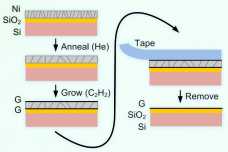 |
| Illustrated here is a new process for making graphene directly on a nonmetal substrate. First, a nickel layer is applied to the material, in this case silicon dioxide (SiO2). Then carbon is deposited on the surface, where it forms layers of graphene above and beneath the SiO2. The top layer of graphene, attached to the nickel, easily peels away using tape (or, for industrial processes, a layer of adhesive material), leaving behind just the lower layer of graphene stuck to the substrate.
Image courtesy of the researchers |
Abstract:
Graphene's promise as a material for new kinds of electronic devices, among other uses, has led researchers around the world to study the material in search of new applications. But one of the biggest limitations to wider use of the strong, lightweight, highly conductive material has been the hurdle of fabrication on an industrial scale.
A new way to make sheets of graphene:Technique might enable advances in display screens, solar cells, or other devices
Cambridge, MA | Posted on May 23rd, 2014Initial work with the carbon material, which forms an atomic-scale mesh and is just a single atom thick, has relied on the use of tiny flakes, typically obtained by quickly removing a piece of sticky tape from a block of graphite � a low-tech system that does not lend itself to manufacturing. Since then, focus has shifted to making graphene films on metal foil, but researchers have faced difficulties in transferring the graphene from the foil to useful substrates.
Now researchers at MIT and the University of Michigan have come up with a way of producing graphene, in a process that lends itself to scaling up, by making graphene directly on materials such as large sheets of glass. The process is described, in a paper published this week in the journal Scientific Reports, by a team of nine researchers led by A. John Hart of MIT. Lead authors of the paper are Dan McNerny, a former MIT postdoc who is now at Michigan, and Viswanath Balakrishnan, a former MIT postdoc who is now at the Indian Institute of Technology.
Currently, most methods of making graphene first grow the material on a film of metal, such as nickel or copper, says Hart, the Mitsui Career Development Associate Professor of Mechanical Engineering. "To make it useful, you have to get it off the metal and onto a substrate, such as a silicon wafer or a polymer sheet, or something larger like a sheet of glass," he says. "But the process of transferring it has become much more frustrating than the process of growing the graphene itself, and can damage and contaminate the graphene."
The new work, Hart says, still uses a metal film as the template � but instead of making graphene only on top of the metal film, it makes graphene on both the film's top and bottom. The substrate in this case is silicon dioxide, a form of glass, with a film of nickel on top of it.
Using chemical vapor deposition (CVD) to deposit a graphene layer on top of the nickel film, Hart says, yields "not only graphene on top [of the nickel layer], but also on the bottom." The nickel film can then be peeled away, leaving just the graphene on top of the nonmetallic substrate.
This way, there's no need for a separate process to attach the graphene to the intended substrate � whether it's a large plate of glass for a display screen, or a thin, flexible material that could be used as the basis for a lightweight, portable solar cell, for example. "You do the CVD on the substrate, and, using our method, the graphene stays behind on the substrate," Hart says.
In addition to the researchers at Michigan, where Hart previously taught, the work was done in collaboration with a large glass manufacturer, Guardian Industries. "To meet their manufacturing needs, it must be very scalable," Hart says. The company currently uses a float process, where glass moves along at a speed of several meters per minute in facilities that produce hundreds of tons of glass every day. "We were inspired by the need to develop a scalable manufacturing process that could produce graphene directly on a glass substrate," Hart says.
The work is still in an early stage; Hart cautions that "we still need to improve the uniformity and the quality of the graphene to make it useful." But the potential is great, he suggests: "The ability to produce graphene directly on nonmetal substrates could be used for large-format displays and touch screens, and for 'smart' windows that have integrated devices like heaters and sensors."
Hart adds that the approach could also be used for small-scale applications, such as integrated circuits on silicon wafers, if graphene can be synthesized at lower temperatures than were used in the present study.
"This new process is based on an understanding of graphene growth in concert with the mechanics of the nickel film," he says. "We've shown this mechanism can work. Now it's a matter of improving the attributes needed to produce a high-performance graphene coating."
###
The work was supported by Guardian Industries, the National Science Foundation, and the Air Force Office of Scientific Research.
Written by David Chandler, MIT News Office
####
For more information, please click here
Contacts:
Andrew Carleen
617-253-1682
Copyright © Massachusetts Institute of Technology
If you have a comment, please Contact us.Issuers of news releases, not 7th Wave, Inc. or Nanotechnology Now, are solely responsible for the accuracy of the content.
Bookmark:


| Related News Press |
News and information
![]() Quantum computer improves AI predictions April 17th, 2026
Quantum computer improves AI predictions April 17th, 2026
![]() Flexible sensor gains sensitivity under pressure April 17th, 2026
Flexible sensor gains sensitivity under pressure April 17th, 2026
![]() A reusable chip for particulate matter sensing April 17th, 2026
A reusable chip for particulate matter sensing April 17th, 2026
![]() Detecting vibrational quantum beating in the predissociation dynamics of SF6 using time-resolved photoelectron spectroscopy April 17th, 2026
Detecting vibrational quantum beating in the predissociation dynamics of SF6 using time-resolved photoelectron spectroscopy April 17th, 2026
Thin films
![]() Tiny nanosheets, big leap: A new sensor detects ethanol at ultra-low levels January 30th, 2026
Tiny nanosheets, big leap: A new sensor detects ethanol at ultra-low levels January 30th, 2026
Display technology/LEDs/SS Lighting/OLEDs
![]() Spinel-type sulfide semiconductors to operate the next-generation LEDs and solar cells For solar-cell absorbers and green-LED source October 3rd, 2025
Spinel-type sulfide semiconductors to operate the next-generation LEDs and solar cells For solar-cell absorbers and green-LED source October 3rd, 2025
Graphene/ Graphite
![]() Electrifying results shed light on graphene foam as a potential material for lab grown cartilage June 6th, 2025
Electrifying results shed light on graphene foam as a potential material for lab grown cartilage June 6th, 2025
![]() Breakthrough in proton barrier films using pore-free graphene oxide: Kumamoto University researchers achieve new milestone in advanced coating technologies September 13th, 2024
Breakthrough in proton barrier films using pore-free graphene oxide: Kumamoto University researchers achieve new milestone in advanced coating technologies September 13th, 2024
Govt.-Legislation/Regulation/Funding/Policy
![]() Quantum computer improves AI predictions April 17th, 2026
Quantum computer improves AI predictions April 17th, 2026
![]() Metasurfaces smooth light to boost magnetic sensing precision January 30th, 2026
Metasurfaces smooth light to boost magnetic sensing precision January 30th, 2026
![]() New imaging approach transforms study of bacterial biofilms August 8th, 2025
New imaging approach transforms study of bacterial biofilms August 8th, 2025
Chip Technology
![]() A reusable chip for particulate matter sensing April 17th, 2026
A reusable chip for particulate matter sensing April 17th, 2026
![]() Metasurfaces smooth light to boost magnetic sensing precision January 30th, 2026
Metasurfaces smooth light to boost magnetic sensing precision January 30th, 2026
Discoveries
![]() Quantum computer improves AI predictions April 17th, 2026
Quantum computer improves AI predictions April 17th, 2026
![]() Flexible sensor gains sensitivity under pressure April 17th, 2026
Flexible sensor gains sensitivity under pressure April 17th, 2026
![]() A reusable chip for particulate matter sensing April 17th, 2026
A reusable chip for particulate matter sensing April 17th, 2026
![]() Detecting vibrational quantum beating in the predissociation dynamics of SF6 using time-resolved photoelectron spectroscopy April 17th, 2026
Detecting vibrational quantum beating in the predissociation dynamics of SF6 using time-resolved photoelectron spectroscopy April 17th, 2026
Materials/Metamaterials/Magnetoresistance
![]() First real-time observation of two-dimensional melting process: Researchers at Mainz University unveil new insights into magnetic vortex structures August 8th, 2025
First real-time observation of two-dimensional melting process: Researchers at Mainz University unveil new insights into magnetic vortex structures August 8th, 2025
![]() Researchers unveil a groundbreaking clay-based solution to capture carbon dioxide and combat climate change June 6th, 2025
Researchers unveil a groundbreaking clay-based solution to capture carbon dioxide and combat climate change June 6th, 2025
![]() A 1960s idea inspires NBI researchers to study hitherto inaccessible quantum states June 6th, 2025
A 1960s idea inspires NBI researchers to study hitherto inaccessible quantum states June 6th, 2025
![]() Institute for Nanoscience hosts annual proposal planning meeting May 16th, 2025
Institute for Nanoscience hosts annual proposal planning meeting May 16th, 2025
Announcements
![]() A fundamentally new therapeutic approach to cystic fibrosis: Nanobody repairs cellular defect April 17th, 2026
A fundamentally new therapeutic approach to cystic fibrosis: Nanobody repairs cellular defect April 17th, 2026
![]() UC Irvine physicists discover method to reverse �quantum scrambling� : The work addresses the problem of information loss in quantum computing system April 17th, 2026
UC Irvine physicists discover method to reverse �quantum scrambling� : The work addresses the problem of information loss in quantum computing system April 17th, 2026
Interviews/Book Reviews/Essays/Reports/Podcasts/Journals/White papers/Posters
![]() A fundamentally new therapeutic approach to cystic fibrosis: Nanobody repairs cellular defect April 17th, 2026
A fundamentally new therapeutic approach to cystic fibrosis: Nanobody repairs cellular defect April 17th, 2026
![]() UC Irvine physicists discover method to reverse �quantum scrambling� : The work addresses the problem of information loss in quantum computing system April 17th, 2026
UC Irvine physicists discover method to reverse �quantum scrambling� : The work addresses the problem of information loss in quantum computing system April 17th, 2026
Military
![]() Quantum engineers �squeeze� laser frequency combs to make more sensitive gas sensors January 17th, 2025
Quantum engineers �squeeze� laser frequency combs to make more sensitive gas sensors January 17th, 2025
![]() Chainmail-like material could be the future of armor: First 2D mechanically interlocked polymer exhibits exceptional flexibility and strength January 17th, 2025
Chainmail-like material could be the future of armor: First 2D mechanically interlocked polymer exhibits exceptional flexibility and strength January 17th, 2025
![]() Single atoms show their true color July 5th, 2024
Single atoms show their true color July 5th, 2024
![]() NRL charters Navy�s quantum inertial navigation path to reduce drift April 5th, 2024
NRL charters Navy�s quantum inertial navigation path to reduce drift April 5th, 2024
Energy
![]() Sensors innovations for smart lithium-based batteries: advancements, opportunities, and potential challenges August 8th, 2025
Sensors innovations for smart lithium-based batteries: advancements, opportunities, and potential challenges August 8th, 2025
![]() Simple algorithm paired with standard imaging tool could predict failure in lithium metal batteries August 8th, 2025
Simple algorithm paired with standard imaging tool could predict failure in lithium metal batteries August 8th, 2025
Industrial
![]() Tiny nanosheets, big leap: A new sensor detects ethanol at ultra-low levels January 30th, 2026
Tiny nanosheets, big leap: A new sensor detects ethanol at ultra-low levels January 30th, 2026
![]() Quantum interference in molecule-surface collisions February 28th, 2025
Quantum interference in molecule-surface collisions February 28th, 2025
![]() Boron nitride nanotube fibers get real: Rice lab creates first heat-tolerant, stable fibers from wet-spinning process June 24th, 2022
Boron nitride nanotube fibers get real: Rice lab creates first heat-tolerant, stable fibers from wet-spinning process June 24th, 2022
Solar/Photovoltaic
![]() Spinel-type sulfide semiconductors to operate the next-generation LEDs and solar cells For solar-cell absorbers and green-LED source October 3rd, 2025
Spinel-type sulfide semiconductors to operate the next-generation LEDs and solar cells For solar-cell absorbers and green-LED source October 3rd, 2025
![]() KAIST researchers introduce new and improved, next-generation perovskite solar cell November 8th, 2024
KAIST researchers introduce new and improved, next-generation perovskite solar cell November 8th, 2024
![]() Groundbreaking precision in single-molecule optoelectronics August 16th, 2024
Groundbreaking precision in single-molecule optoelectronics August 16th, 2024
![]() Development of zinc oxide nanopagoda array photoelectrode: photoelectrochemical water-splitting hydrogen production January 12th, 2024
Development of zinc oxide nanopagoda array photoelectrode: photoelectrochemical water-splitting hydrogen production January 12th, 2024
|
|
||
|
|
||
| The latest news from around the world, FREE | ||
|
|
||
|
|
||
| Premium Products | ||
|
|
||
|
Only the news you want to read!
Learn More |
||
|
|
||
|
Full-service, expert consulting
Learn More |
||
|
|
||