Home > Press > Probing dopant distribution: Finding by Berkeley Lab Researchers at the Molecular Foundry Opens the Door to Better Doping of Semiconductor Nanocrystals
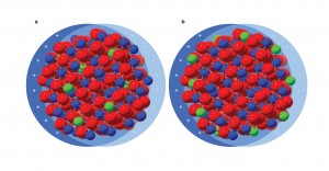 |
| Schematic representation of plasmonic nanocrystals with (a) uniform and (b) surface-segregated dopant distributions. In (a), most of the electron cloud is scattered from ionized impurities (green); in (b), most of the electron cloud is oscillating away from the impurities. |
Abstract:
The icing on the cake for semiconductor nanocrystals that provide a non-damped optoelectronic effect may exist as a layer of tin that segregates near the surface.
Probing dopant distribution: Finding by Berkeley Lab Researchers at the Molecular Foundry Opens the Door to Better Doping of Semiconductor Nanocrystals
Berkeley, CA | Posted on May 7th, 2014One method of altering the electrical properties of a semiconductor is by introducing impurities called dopants. A team led by Delia Milliron, a chemist at Berkeley Lab's Molecular Foundry, a U.S Department of Energy (DOE) national nanoscience center, has demonstrated that equally important as the amount of dopant is how the dopant is distributed on the surface and throughout the material. This opens the door for engineering the distribution of the dopant in order to control what wavelength the material will absorb and more generally how light interacts with the nanocrystals.
"Doping in semiconductor nanocrystals is still an evolving art," says Milliron. "Only in the last few years have people begun to observe interesting optical properties as a result of introducing dopants to these materials, but how the dopants are distributed within the nanocrystals remains largely unknown. What sites they occupy and where they are situated throughout the material greatly influences optical properties."
Milliron's most recent claim to fame, a "smart window" technology that not only blocks natural infrared (IR) radiation while allowing the passage of visible light through transparent coated glass, but also allows for independent control over both kinds of radiation, relies on a doped semiconductor called indium tin oxide (ITO).
ITO, in which tin (the dopant) has replaced some of the indium ions in indium oxide (the semiconductor), has become the prototypical doped semiconductor nanocrystal material. It is used in all kinds of electronic devices, including touchscreens displays, smart windows and solar cells.
"The exciting thing about this class of materials is that the dopants are able to introduce free electrons that form at high density within the material, which makes them conducting and thus useful as transparent conductors," says Milliron
But the same electrons cause the materials to be plasmonic in the IR part of the spectrum. This means that light of IR wavelength can be resonant with free electrons in the material: the oscillating electric fields in the light resonate and can cause absorption.
"[These materials] can absorb IR light in a way that's tunable by adjusting the doping, while still being transparent to natural visible light. A tunable amount of absorption of IR light allows you to control heating. For us, that's the driving application," explains Milliron.
Until now, adjustments have been made by changing the amount of dopant in the semiconductor. Puzzled by studies in which optical properties did not behave as expected, Milliron and University of California (UC) Berkeley PhD candidate Sebastien Lounis looked to x-ray photoelectron spectroscopy to probe electrons near the surface of the ITO samples and investigate the distribution of elements within the samples at the Stanford Synchrotron Radiation Lightsource (SSRL).
The SSRL uses a tuneable beam of photons to excite electrons inside the material. If the electrons are close enough to the surface, they can sometimes be emitted and collected by a detector. These electrons provide information about the properties of the material, including the ratio of the amounts of different elements like indium and tin in ITO. Increasing the energy of the x-ray beam shows how the composition of tin and indium changes as one moves deeper into the sample. Ultimately, the spectroscopy technique allowed Milliron and her team to probe the doping distribution as a function of distance from the nanocrystals' surface.
Studies of two sets of samples allowed them to correlated tin distribution with optical properties, and showed that the shape and wavelength of plasmon absorption depended on tin distribution. The tin segregated on the surface showed reduced activation of dopants and symmetric plasmon resonances, with no damping caused by the dopants.
"When the tin sits near the surface, it interacts only weakly with the majority of the free electrons," explains Lounis. "This gives us the benefits of doping without some of drawbacks."
"Now that we know how to probe, we can go after targeted design features for particular applications," concludes Milliron. Deliberate placement of dopants by design provides a new tool for "dialing in plasmonic materials to do exactly what we want in terms of interaction with light."
A paper on this research has been accepted for publication in the Journal of the American Chemical Society (JACS) in April 2014. The paper is titled "The influence of dopant distribution on the plasmonic properties of indium tin oxide nanocrystals" with Lounis as the lead author and Milliron as the corresponding author. Other authors are Evan Runnerstorm, Amy Bergerud, and Dennis Nordlund.
This research was primarily supported by the DOE Office of Science.
####
About DOE/Lawrence Berkeley National Laboratory
Lawrence Berkeley National Laboratory addresses the world�s most urgent scientific challenges by advancing sustainable energy, protecting human health, creating new materials, and revealing the origin and fate of the universe. Founded in 1931, Berkeley Lab�s scientific expertise has been recognized with 13 Nobel prizes. The University of California manages Berkeley Lab for the U.S. Department of Energy�s Office of Science. For more, visit www.lbl.gov.
For more information, please click here
Contacts:
Rachel Berkowitz
(510) 486-7254
Copyright © DOE/Lawrence Berkeley National Laboratory
If you have a comment, please Contact us.Issuers of news releases, not 7th Wave, Inc. or Nanotechnology Now, are solely responsible for the accuracy of the content.
Bookmark:


| Related Links |
| Related News Press |
News and information
![]() Quantum computer improves AI predictions April 17th, 2026
Quantum computer improves AI predictions April 17th, 2026
![]() Flexible sensor gains sensitivity under pressure April 17th, 2026
Flexible sensor gains sensitivity under pressure April 17th, 2026
![]() A reusable chip for particulate matter sensing April 17th, 2026
A reusable chip for particulate matter sensing April 17th, 2026
![]() Detecting vibrational quantum beating in the predissociation dynamics of SF6 using time-resolved photoelectron spectroscopy April 17th, 2026
Detecting vibrational quantum beating in the predissociation dynamics of SF6 using time-resolved photoelectron spectroscopy April 17th, 2026
Physics
![]() UC Irvine physicists discover method to reverse �quantum scrambling� : The work addresses the problem of information loss in quantum computing system April 17th, 2026
UC Irvine physicists discover method to reverse �quantum scrambling� : The work addresses the problem of information loss in quantum computing system April 17th, 2026
Chemistry
![]() Projecting light to dispense liquids: A new route to ultra-precise microdroplets January 30th, 2026
Projecting light to dispense liquids: A new route to ultra-precise microdroplets January 30th, 2026
![]() From sensors to smart systems: the rise of AI-driven photonic noses January 30th, 2026
From sensors to smart systems: the rise of AI-driven photonic noses January 30th, 2026
![]() "Nanoreactor" cage uses visible light for catalytic and ultra-selective cross-cycloadditions October 3rd, 2025
"Nanoreactor" cage uses visible light for catalytic and ultra-selective cross-cycloadditions October 3rd, 2025
![]() Cambridge chemists discover simple way to build bigger molecules � one carbon at a time June 6th, 2025
Cambridge chemists discover simple way to build bigger molecules � one carbon at a time June 6th, 2025
Laboratories
![]() Researchers develop molecular qubits that communicate at telecom frequencies October 3rd, 2025
Researchers develop molecular qubits that communicate at telecom frequencies October 3rd, 2025
Govt.-Legislation/Regulation/Funding/Policy
![]() Quantum computer improves AI predictions April 17th, 2026
Quantum computer improves AI predictions April 17th, 2026
![]() Metasurfaces smooth light to boost magnetic sensing precision January 30th, 2026
Metasurfaces smooth light to boost magnetic sensing precision January 30th, 2026
![]() New imaging approach transforms study of bacterial biofilms August 8th, 2025
New imaging approach transforms study of bacterial biofilms August 8th, 2025
Chip Technology
![]() A reusable chip for particulate matter sensing April 17th, 2026
A reusable chip for particulate matter sensing April 17th, 2026
![]() Metasurfaces smooth light to boost magnetic sensing precision January 30th, 2026
Metasurfaces smooth light to boost magnetic sensing precision January 30th, 2026
Discoveries
![]() Quantum computer improves AI predictions April 17th, 2026
Quantum computer improves AI predictions April 17th, 2026
![]() Flexible sensor gains sensitivity under pressure April 17th, 2026
Flexible sensor gains sensitivity under pressure April 17th, 2026
![]() A reusable chip for particulate matter sensing April 17th, 2026
A reusable chip for particulate matter sensing April 17th, 2026
![]() Detecting vibrational quantum beating in the predissociation dynamics of SF6 using time-resolved photoelectron spectroscopy April 17th, 2026
Detecting vibrational quantum beating in the predissociation dynamics of SF6 using time-resolved photoelectron spectroscopy April 17th, 2026
Materials/Metamaterials/Magnetoresistance
![]() First real-time observation of two-dimensional melting process: Researchers at Mainz University unveil new insights into magnetic vortex structures August 8th, 2025
First real-time observation of two-dimensional melting process: Researchers at Mainz University unveil new insights into magnetic vortex structures August 8th, 2025
![]() Researchers unveil a groundbreaking clay-based solution to capture carbon dioxide and combat climate change June 6th, 2025
Researchers unveil a groundbreaking clay-based solution to capture carbon dioxide and combat climate change June 6th, 2025
![]() A 1960s idea inspires NBI researchers to study hitherto inaccessible quantum states June 6th, 2025
A 1960s idea inspires NBI researchers to study hitherto inaccessible quantum states June 6th, 2025
![]() Institute for Nanoscience hosts annual proposal planning meeting May 16th, 2025
Institute for Nanoscience hosts annual proposal planning meeting May 16th, 2025
Announcements
![]() A fundamentally new therapeutic approach to cystic fibrosis: Nanobody repairs cellular defect April 17th, 2026
A fundamentally new therapeutic approach to cystic fibrosis: Nanobody repairs cellular defect April 17th, 2026
![]() UC Irvine physicists discover method to reverse �quantum scrambling� : The work addresses the problem of information loss in quantum computing system April 17th, 2026
UC Irvine physicists discover method to reverse �quantum scrambling� : The work addresses the problem of information loss in quantum computing system April 17th, 2026
Interviews/Book Reviews/Essays/Reports/Podcasts/Journals/White papers/Posters
![]() A fundamentally new therapeutic approach to cystic fibrosis: Nanobody repairs cellular defect April 17th, 2026
A fundamentally new therapeutic approach to cystic fibrosis: Nanobody repairs cellular defect April 17th, 2026
![]() UC Irvine physicists discover method to reverse �quantum scrambling� : The work addresses the problem of information loss in quantum computing system April 17th, 2026
UC Irvine physicists discover method to reverse �quantum scrambling� : The work addresses the problem of information loss in quantum computing system April 17th, 2026
Energy
![]() Sensors innovations for smart lithium-based batteries: advancements, opportunities, and potential challenges August 8th, 2025
Sensors innovations for smart lithium-based batteries: advancements, opportunities, and potential challenges August 8th, 2025
![]() Simple algorithm paired with standard imaging tool could predict failure in lithium metal batteries August 8th, 2025
Simple algorithm paired with standard imaging tool could predict failure in lithium metal batteries August 8th, 2025
|
|
||
|
|
||
| The latest news from around the world, FREE | ||
|
|
||
|
|
||
| Premium Products | ||
|
|
||
|
Only the news you want to read!
Learn More |
||
|
|
||
|
Full-service, expert consulting
Learn More |
||
|
|
||