Home > Press > Playing pool with carbon atoms: UA physicists discover how to change the crystal structure of graphene
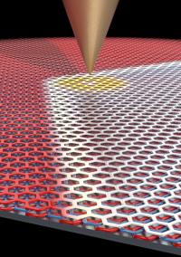 |
| Using a sharp metal scanning tunneling microscopy tip, LeRoy and his collaborators were able to move the domain border between the two graphene configurations around.
Credit: Pablo San-Jose ICMM-CSI |
Abstract:
A University of Arizona-led team of physicists has discovered how to change the crystal structure of graphene, more commonly known as pencil lead, with an electric field, an important step toward the possible use of graphene in microprocessors that would be smaller and faster than current, silicon-based technology.
Playing pool with carbon atoms: UA physicists discover how to change the crystal structure of graphene
Tucson, AZ | Posted on April 30th, 2014Graphene consists of extremely thin sheets of graphite: when writing with a pencil, graphene sheets slough off the pencil's graphite core and stick to the page. If placed under a high-powered electron microscope, graphene reveals its sheet-like structure of cross-linked carbon atoms, resembling chicken wire.
When manipulated by an electric field, parts of the material are transformed from behaving as a metal to behaving as a semiconductor, the UA physicists found.
Graphene is the world's thinnest material, with 300,000 sheets needed to amount to the thickness of a human hair or a sheet of paper. Scientists and engineers are interested in it because of its possible applications in microelectronic devices, in hopes of propelling us from the silicon age to the graphene age. The tricky part is to control the flow of electrons through the material, a necessary prerequisite for putting it to work in any type of electronic circuit.
Brian LeRoy, UA associate professor of physics, and his collaborators have cleared a hurdle toward that goal by showing that an electric field is capable of controlling the crystal structure of trilayer graphene - which is made up of three layers of graphene.
Most materials require high temperatures, pressure or both to change their crystal structure, which is the reason why graphite doesn't spontaneously turn into diamond or vice versa.
"It is extremely rare for a material to change its crystal structure just by applying an electric field," LeRoy said. "Making trilayer graphene is an exceptionally unique system that could be utilized to create novel devices."
Trilayer graphene can be stacked in two unique ways. This is analogous to stacking layers of billiards balls in a triangular lattice, with the balls representing the carbon atoms.
"When you stack two layers of billiards balls, their 'crystal structure' is fixed because the top layer of balls must sit in holes formed by the triangles of the bottom layer," explained Matthew Yankowitz, a third-year doctoral student in LeRoy's lab. He is the first author on the published research, which appears in the journal Nature Materials. "The third layer of balls may be stacked in such a way that its balls are flush above the balls in the bottom layer, or it may be offset slightly so its balls come to lie above the holes formed by triangles in the bottom layer."
These two stacking configurations can naturally exist in the same flake of graphene. The two domains are separated by a sharp boundary where the carbon hexagons are strained to accommodate the transition from one stacking pattern to the other.
"Due to the different stacking configurations on either side of the domain wall, one side of the material behaves as a metal, while the other side behaves as a semiconductor," LeRoy explained.
While probing the domain wall with an electric field, applied by an extremely sharp metal scanning tunneling microscopy tip, the researchers in LeRoy's group discovered that they could move the position of the domain wall within the flake of graphene. And as they moved the domain wall, the crystal structure of the trilayer graphene changed in its wake.
"We had the idea that there would be interesting electronic effects at the boundary, and the boundary kept moving around on us," LeRoy said. "At first it was frustrating, but once we realized what was going on, it turned out to be the most interesting effect."
By applying an electric field to move the boundary, it is now possible for the first time to change the crystal structure of graphene in a controlled fashion.
"Now we have a knob that we can turn to change the material from metallic into semiconducting and vice versa to control the flow of electrons," LeRoy said. "It basically gives us an on-off switch, which had not been realized yet in graphene."
While more research is needed before graphene can be applied in technological applications on an industrial scale, researchers see ways it may be used.
"If you used a wide electrode instead of a pointed tip, you could move the boundary between the two configurations a farther distance, which could make it possible to create transistors from graphene," Yankowitz said.
Transistors are a staple of electronic circuits because they control the flow of electrons.
Unlike silicon transistors used now, graphene-based transistors could be extremely thin, making the device much smaller, and since electrons move through graphene much faster than through silicon, the devices would enable faster computing.
In addition, silicon-based transistors are being manufactured to function as one of two types - p-type or n-type - whereas graphene could operate as both. This would make them cheaper to produce and more versatile in their applications.
###
The other contributors to the research paper, "Electric field control of soliton motion and stacking in trilayer graphene," include Joel I-Jan Wang (Massachusetts Institute of Technology and Harvard University in Cambridge, Massachusetts), A. Glen Birdwell (U.S. Army Research Laboratory, Adelphi, Maryland), Yu-An Chen (MIT), K. Watanabe and T. Taniguchi (National Institute for Materials Science, Tsukuba, Japan), Philippe Jacquod (UA Department of Physics), Pablo San-Jose (Instituto de Ciencia de Materiales de Madrid) and Pablo Jarillo-Herrero (MIT).
####
For more information, please click here
Contacts:
Daniel Stolte
520-626-4402
Copyright © University of Arizona
If you have a comment, please Contact us.Issuers of news releases, not 7th Wave, Inc. or Nanotechnology Now, are solely responsible for the accuracy of the content.
Bookmark:


| Related Links |
![]() The study appears in the advance online publication of Nature Materials at:
The study appears in the advance online publication of Nature Materials at:
| Related News Press |
News and information
![]() Quantum computer improves AI predictions April 17th, 2026
Quantum computer improves AI predictions April 17th, 2026
![]() Flexible sensor gains sensitivity under pressure April 17th, 2026
Flexible sensor gains sensitivity under pressure April 17th, 2026
![]() A reusable chip for particulate matter sensing April 17th, 2026
A reusable chip for particulate matter sensing April 17th, 2026
![]() Detecting vibrational quantum beating in the predissociation dynamics of SF6 using time-resolved photoelectron spectroscopy April 17th, 2026
Detecting vibrational quantum beating in the predissociation dynamics of SF6 using time-resolved photoelectron spectroscopy April 17th, 2026
Laboratories
![]() Researchers develop molecular qubits that communicate at telecom frequencies October 3rd, 2025
Researchers develop molecular qubits that communicate at telecom frequencies October 3rd, 2025
Graphene/ Graphite
![]() Electrifying results shed light on graphene foam as a potential material for lab grown cartilage June 6th, 2025
Electrifying results shed light on graphene foam as a potential material for lab grown cartilage June 6th, 2025
![]() Breakthrough in proton barrier films using pore-free graphene oxide: Kumamoto University researchers achieve new milestone in advanced coating technologies September 13th, 2024
Breakthrough in proton barrier films using pore-free graphene oxide: Kumamoto University researchers achieve new milestone in advanced coating technologies September 13th, 2024
Govt.-Legislation/Regulation/Funding/Policy
![]() Quantum computer improves AI predictions April 17th, 2026
Quantum computer improves AI predictions April 17th, 2026
![]() Metasurfaces smooth light to boost magnetic sensing precision January 30th, 2026
Metasurfaces smooth light to boost magnetic sensing precision January 30th, 2026
![]() New imaging approach transforms study of bacterial biofilms August 8th, 2025
New imaging approach transforms study of bacterial biofilms August 8th, 2025
Chip Technology
![]() A reusable chip for particulate matter sensing April 17th, 2026
A reusable chip for particulate matter sensing April 17th, 2026
![]() Metasurfaces smooth light to boost magnetic sensing precision January 30th, 2026
Metasurfaces smooth light to boost magnetic sensing precision January 30th, 2026
Discoveries
![]() Quantum computer improves AI predictions April 17th, 2026
Quantum computer improves AI predictions April 17th, 2026
![]() Flexible sensor gains sensitivity under pressure April 17th, 2026
Flexible sensor gains sensitivity under pressure April 17th, 2026
![]() A reusable chip for particulate matter sensing April 17th, 2026
A reusable chip for particulate matter sensing April 17th, 2026
![]() Detecting vibrational quantum beating in the predissociation dynamics of SF6 using time-resolved photoelectron spectroscopy April 17th, 2026
Detecting vibrational quantum beating in the predissociation dynamics of SF6 using time-resolved photoelectron spectroscopy April 17th, 2026
Announcements
![]() A fundamentally new therapeutic approach to cystic fibrosis: Nanobody repairs cellular defect April 17th, 2026
A fundamentally new therapeutic approach to cystic fibrosis: Nanobody repairs cellular defect April 17th, 2026
![]() UC Irvine physicists discover method to reverse �quantum scrambling� : The work addresses the problem of information loss in quantum computing system April 17th, 2026
UC Irvine physicists discover method to reverse �quantum scrambling� : The work addresses the problem of information loss in quantum computing system April 17th, 2026
Interviews/Book Reviews/Essays/Reports/Podcasts/Journals/White papers/Posters
![]() A fundamentally new therapeutic approach to cystic fibrosis: Nanobody repairs cellular defect April 17th, 2026
A fundamentally new therapeutic approach to cystic fibrosis: Nanobody repairs cellular defect April 17th, 2026
![]() UC Irvine physicists discover method to reverse �quantum scrambling� : The work addresses the problem of information loss in quantum computing system April 17th, 2026
UC Irvine physicists discover method to reverse �quantum scrambling� : The work addresses the problem of information loss in quantum computing system April 17th, 2026
Tools
![]() Metasurfaces smooth light to boost magnetic sensing precision January 30th, 2026
Metasurfaces smooth light to boost magnetic sensing precision January 30th, 2026
![]() From sensors to smart systems: the rise of AI-driven photonic noses January 30th, 2026
From sensors to smart systems: the rise of AI-driven photonic noses January 30th, 2026
![]() Japan launches fully domestically produced quantum computer: Expo visitors to experience quantum computing firsthand August 8th, 2025
Japan launches fully domestically produced quantum computer: Expo visitors to experience quantum computing firsthand August 8th, 2025
Military
![]() Quantum engineers �squeeze� laser frequency combs to make more sensitive gas sensors January 17th, 2025
Quantum engineers �squeeze� laser frequency combs to make more sensitive gas sensors January 17th, 2025
![]() Chainmail-like material could be the future of armor: First 2D mechanically interlocked polymer exhibits exceptional flexibility and strength January 17th, 2025
Chainmail-like material could be the future of armor: First 2D mechanically interlocked polymer exhibits exceptional flexibility and strength January 17th, 2025
![]() Single atoms show their true color July 5th, 2024
Single atoms show their true color July 5th, 2024
![]() NRL charters Navy�s quantum inertial navigation path to reduce drift April 5th, 2024
NRL charters Navy�s quantum inertial navigation path to reduce drift April 5th, 2024
Research partnerships
![]() Lab to industry: InSe wafer-scale breakthrough for future electronics August 8th, 2025
Lab to industry: InSe wafer-scale breakthrough for future electronics August 8th, 2025
![]() HKU physicists uncover hidden order in the quantum world through deconfined quantum critical points April 25th, 2025
HKU physicists uncover hidden order in the quantum world through deconfined quantum critical points April 25th, 2025
|
|
||
|
|
||
| The latest news from around the world, FREE | ||
|
|
||
|
|
||
| Premium Products | ||
|
|
||
|
Only the news you want to read!
Learn More |
||
|
|
||
|
Full-service, expert consulting
Learn More |
||
|
|
||