Home > Press > Unavoidable disorder used to build nanolaser
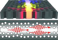 |
| The nanolaser is based on the disorder in the pattern of holes in the photonic crystal. The light source is built into the photonic crystal itself, which is clear as glass and when the light hits a hole it is reflected and is channeled into the so-called waveguide, the crystal's middle lane. But the light is thrown back and forth in the photonic crystal and due to imperfections is intensified and spontaneously turns into laser light.
Credit: Quantum Photonics, Niels Bohr Institute |
Abstract:
Researchers the world round are working to develop optical chips, where light can be controlled with nanostructures. These could be used for future circuits based on light (photons) instead of electron - that is photonics instead of electronics. But it has proved to be impossible to achieve perfect photonic nanostructures: they are inevitably a little bit imperfect. Now researchers at the Niels Bohr Institute in collaboration with DTU have discovered that imperfect nanostructures can offer entirely new functionalities. They have shown that imperfect optical chips can be used to produce 'nanolasers', which is an ultimately compact and energy-efficient light source. The results are published in the scientific journal Nature Nanotechnology.
Unavoidable disorder used to build nanolaser
Copenhagen, Denmark | Posted on March 25th, 2014The researchers are working with extremely small photonic crystal membranes - the width of the membrane is 25 micrometer (1 micrometer is one thousandth of a millimeter), and the thickness is 340 nanometers (1 nanometer is one thousandth of a micrometer). The crystals are made of the semiconducting material gallium arsenide (GaAs). A pattern of holes are etched into the material at a regular distance of 380 nanometers. The holes have the function of acting as built-in mirrors that reflect the light and can thus be used to control the spread of the light in the optical chip. The researchers have therefore tried to achieve as perfect a regular structure of holes as possible to control the light in certain optical circuit.
Unavoidable disorder exploited
But in practice it is impossible to avoid small irregularities during the manufacture of the optical chips and this can be a big problem, as it can result in the loss of light and therefore reduced functionality. Researchers at the Niels Bohr Institute have now turned the problem of imperfections into an advantage.
"It turns out that the imperfect optical chips are extremely well suited for capturing light. When the light is sent into the imperfect chip, it will hit the many small irregular holes, which reflect the light in random directions. Due to the frequent reflections, the light is spontaneously captured in the nanostructure and cannot escape. This allows the light to be amplified, resulting in surprisingly good conditions for creating highly efficient and compact lasers," explains Peter Lodahl, professor and head of the Quantum Photonic research group at the Niels Bohr Institute at the University of Copenhagen.
Experiment with built-in light
The researchers in Quantum Photonics at the Niels Bohr Institute, led by Professor Peter Lodahl and Associate Professor S�ren Stobbe, designed the photonic crystal and carried out the experimental studies in the research group's laboratories.
The light source is integrated into the photonic crystal itself and is comprised of a layer of artificial atoms that emit light (the basic component of light is photons). The photons are sent through the crystal, which is clear as glass and has a pattern of tiny holes. When a photon hits a hole it is reflected and channeled into the so-called waveguide, which is a 'photon track' that can be used to guide the photons through the photonic crystal. However, due to the imperfect holes the light will be thrown back and forth in the waveguide of the photonic crystal, intensifying it and turning it into laser light.
The result is laser light on a nanometer scale and the researchers see great potential in this.
The dream of a quantum Internet
"The fact that we can control the light and produce laser light on a nanometer scale can be used to create circuits based on photons instead of electrons, thus paving the way for optical quantum communication technology in the future. With built-in laser sources, we will be able to integrate optical components and it allows for the building of complex functionalities. Our ultimate dream is to build a 'quantum internet', where the informations is coded in individual photons," explain Peter Lodahl and S�ren Stobbe, who are excited about the results, which show that the unavoidable disorder in optical chip is not a limitation and can even be exploited under the right conditions.
####
For more information, please click here
Contacts:
Gertie Skaarup
45-28-75-06-20
Peter Lodahl
Professor
Quantum Photonics
Niels Bohr Institute
University of Copenhagen
+45 2056-5303
http://www.quantum-photonics.dk
S�ren Stobbe
Associate Professor
Quantum Photonics
Niels Bohr Institute
University of Copenhagen
+45 3532-5216
http://www.quantum-photonics.dk
Copyright © University of Copenhagen - Niels Bohr Institute
If you have a comment, please Contact us.Issuers of news releases, not 7th Wave, Inc. or Nanotechnology Now, are solely responsible for the accuracy of the content.
Bookmark:


| Related News Press |
News and information
![]() Quantum computer improves AI predictions April 17th, 2026
Quantum computer improves AI predictions April 17th, 2026
![]() Flexible sensor gains sensitivity under pressure April 17th, 2026
Flexible sensor gains sensitivity under pressure April 17th, 2026
![]() A reusable chip for particulate matter sensing April 17th, 2026
A reusable chip for particulate matter sensing April 17th, 2026
![]() Detecting vibrational quantum beating in the predissociation dynamics of SF6 using time-resolved photoelectron spectroscopy April 17th, 2026
Detecting vibrational quantum beating in the predissociation dynamics of SF6 using time-resolved photoelectron spectroscopy April 17th, 2026
Display technology/LEDs/SS Lighting/OLEDs
![]() Spinel-type sulfide semiconductors to operate the next-generation LEDs and solar cells For solar-cell absorbers and green-LED source October 3rd, 2025
Spinel-type sulfide semiconductors to operate the next-generation LEDs and solar cells For solar-cell absorbers and green-LED source October 3rd, 2025
![]() Efficient and stable hybrid perovskite-organic light-emitting diodes with external quantum efficiency exceeding 40 per cent July 5th, 2024
Efficient and stable hybrid perovskite-organic light-emitting diodes with external quantum efficiency exceeding 40 per cent July 5th, 2024
Chip Technology
![]() A reusable chip for particulate matter sensing April 17th, 2026
A reusable chip for particulate matter sensing April 17th, 2026
![]() Metasurfaces smooth light to boost magnetic sensing precision January 30th, 2026
Metasurfaces smooth light to boost magnetic sensing precision January 30th, 2026
Optical computing/Photonic computing
![]() ICFO researchers overcome long-standing bottleneck in single photon detection with twisted 2D materials August 8th, 2025
ICFO researchers overcome long-standing bottleneck in single photon detection with twisted 2D materials August 8th, 2025
![]() Programmable electron-induced color router array May 14th, 2025
Programmable electron-induced color router array May 14th, 2025
Discoveries
![]() Quantum computer improves AI predictions April 17th, 2026
Quantum computer improves AI predictions April 17th, 2026
![]() Flexible sensor gains sensitivity under pressure April 17th, 2026
Flexible sensor gains sensitivity under pressure April 17th, 2026
![]() A reusable chip for particulate matter sensing April 17th, 2026
A reusable chip for particulate matter sensing April 17th, 2026
![]() Detecting vibrational quantum beating in the predissociation dynamics of SF6 using time-resolved photoelectron spectroscopy April 17th, 2026
Detecting vibrational quantum beating in the predissociation dynamics of SF6 using time-resolved photoelectron spectroscopy April 17th, 2026
Announcements
![]() A fundamentally new therapeutic approach to cystic fibrosis: Nanobody repairs cellular defect April 17th, 2026
A fundamentally new therapeutic approach to cystic fibrosis: Nanobody repairs cellular defect April 17th, 2026
![]() UC Irvine physicists discover method to reverse �quantum scrambling� : The work addresses the problem of information loss in quantum computing system April 17th, 2026
UC Irvine physicists discover method to reverse �quantum scrambling� : The work addresses the problem of information loss in quantum computing system April 17th, 2026
Interviews/Book Reviews/Essays/Reports/Podcasts/Journals/White papers/Posters
![]() A fundamentally new therapeutic approach to cystic fibrosis: Nanobody repairs cellular defect April 17th, 2026
A fundamentally new therapeutic approach to cystic fibrosis: Nanobody repairs cellular defect April 17th, 2026
![]() UC Irvine physicists discover method to reverse �quantum scrambling� : The work addresses the problem of information loss in quantum computing system April 17th, 2026
UC Irvine physicists discover method to reverse �quantum scrambling� : The work addresses the problem of information loss in quantum computing system April 17th, 2026
Photonics/Optics/Lasers
![]() Metasurfaces smooth light to boost magnetic sensing precision January 30th, 2026
Metasurfaces smooth light to boost magnetic sensing precision January 30th, 2026
![]() From sensors to smart systems: the rise of AI-driven photonic noses January 30th, 2026
From sensors to smart systems: the rise of AI-driven photonic noses January 30th, 2026
|
|
||
|
|
||
| The latest news from around the world, FREE | ||
|
|
||
|
|
||
| Premium Products | ||
|
|
||
|
Only the news you want to read!
Learn More |
||
|
|
||
|
Full-service, expert consulting
Learn More |
||
|
|
||