Home > Press > Laser light at useful wavelengths from semiconductor nanowires: Nanowire lasers could work with silicon chips, optical fibers, even living cells
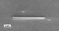 |
| TUM researchers have demonstrated that semiconductor nanowires like the one shown here can act both as lasers, generating coherent pulses of light, and as waveguides, similar to optical fibers. Because these nanowire lasers emit light at technologically useful wavelengths, can be grown on silicon substrates, and operate at room temperature, they have potential for applications in computing, communications, and sensing.
Credit: WSI/TUM |
Abstract:
Thread-like semiconductor structures called nanowires, so thin that they are effectively one-dimensional, show potential as lasers for applications in computing, communications, and sensing. Scientists at the Technische Universitaet Muenchen (TUM) have demonstrated laser action in semiconductor nanowires that emit light at technologically useful wavelengths and operate at room temperature. They now have documented this breakthrough in the journal Nature Communications and, in Nano Letters, have disclosed further results showing enhanced optical and electronic performance.
Laser light at useful wavelengths from semiconductor nanowires: Nanowire lasers could work with silicon chips, optical fibers, even living cells
Muenchen, Germany | Posted on December 5th, 2013"Nanowire lasers could represent the next step in the development of smaller, faster, more energy-efficient sources of light," says Prof. Jonathan Finley, director of TUM's Walter Schottky Institute. Potential applications include on-chip optical interconnects or even optical transistors to speed up computers, integrated optoelectronics for fiber-optic communications, and laser arrays with steerable beams. "But nanowires are also a bit special," Finley adds, "in that they are very sensitive to their surroundings, have a large surface-to-volume ratio, and are small enough, for example, to poke into a biological cell." Thus nanowire lasers could also prove useful in environmental and biological sensing.
These experimental nanowire lasers emit light in the near-infrared, approaching the "sweet spot" for fiber-optic communications. They can be grown directly on silicon, presenting opportunities for integrated photonics and optoelectronics. And they operate at room temperature, a prerequisite for real-world applications.
Tailored in the lab, with an eye toward industry
Tiny as they are - a thousand times thinner than a human hair - the nanowire lasers demonstrated at TUM have a complex "core-shell" cross-section with a profile of differing semiconductor materials tailored virtually atom by atom.
The nanowires' tailored core-shell structure enables them to act both as lasers, generating coherent pulses of light, and as waveguides, similar to optical fibers. Like conventional communication lasers, these nanowires are made of so-called III-V semiconductors, materials with the right "bandgap" to emit light in the near-infrared. A unique advantage, Finley explains, is that the nanowire geometry is "more forgiving than bulk crystals or films, allowing you to combine materials that you normally can't combine." Because the nanowires arise from a base only tens to hundreds of nanometers in diameter, they can be grown directly on silicon chips in a way that alleviates restrictions due to crystal lattice mismatch - thus yielding high-quality material with the potential for high performance.
Put these characteristics together, and it becomes possible to imagine a path from applied research to a variety of future applications. A number of significant challenges remain, however. For example, laser emission from the TUM nanowires was stimulated by light - as were the nanowire lasers reported almost simultaneously by a team at the Australian National University - yet practical applications are likely to require electrically injected devices.
Nanowire lasers: a technological frontier with bright prospects
The newly published results are largely due to a team of scientists who are beginning their careers, under the guidance of Dr. Gregor Koblmueller and other senior researchers, at the frontier of a new field. Doctoral candidates including Benedikt Mayer, Daniel Rudolph, Stefanie Mork�tter and Julian Treu combined their efforts, working together on photonic design, material growth, and characterization using electron microscopy with atomic resolution.
Ongoing research is directed toward better understanding the physical phenomena at work in such devices as well as toward creating electrically injected nanowire lasers, optimizing their performance, and integrating them with platforms for silicon photonics.
"At present very few labs in the world have the capability to grow nanowire materials and devices with the precision required," says co-author Prof. Gerhard Abstreiter, founder of the Walter Schottky Institute and director of the TUM Institute for Advanced Study. "And yet," he explains, "our processes and designs are compatible with industrial production methods for computing and communications. Experience shows that today's hero experiment can become tomorrow's commercial technology, and often does."
###
This research was supported in part by the German Excellence Initiative through the TUM Institute for Advanced Study and the Excellence Cluster Nanosystems Initiative Munich (NIM); by the German Research Foundation (DFG) through Collaborative Research Center SFB 631; by the European Union through a Marie Curie European Reintegration Grant, the QUROPE project SOLID, and the EU-MC network INDEX; by a CINECA award under the ISCRA initiative; and by a grant from Generalitat Valenciana.
Publications:
Lasing from individual GaAs-AlGaAs core-shell nanowires up to room temperature. Benedikt Mayer, Daniel Rudolph, Joscha Schnell, Stefanie Morkoetter, Julia Winnerl, Julian Treu, Kai Mueller, Gregor Bracher, Gerhard Abstreiter, Gregor Koblmueller, and Jonathan J. Finley. Nature Communications, 5 Dec. 2013. DOI: 10.1038/ncomms3931
High mobility one- and two-dimensional electron systems in nanowire-based quantum heterostructures. Stefan Funk, Miguel Royo, Ilaria Zardo, Daniel Rudolph, Stefanie Morkoetter, Benedikt Mayer, Jonathan Becker, Alexander Bechtold, Sonja Matich, Markus Doeblinger, Max Bichler, G. Koblmueller, Jonathan J. Finley, Andrea Bertoni, Guido Goldoni, and Gerhard Abstreiter. Nano Letters Just Accepted Manuscript, 25 Nov. 2013. DOI: dx.doi.org/10.1021/nl403561w
Enhanced luminescence properties of InAs-InAsP core-shell nanowires. Julian Treu, Michael Bormann, Hannes Schmeiduch, Markus Doeblinger, Stefanie Morkoetter, Sonja Matich, Peter Wiecha, Kai Saller, Benedikt Mayer, Max Bichler, Markus Christian Amann, Jonathan Finley, Gerhard Abstreiter, and G. Koblmueller. Nano Letters Just Accepted Manuscript, 25 Nov. 2013. DOI: dx.doi.org/10.1021/nl403341x
####
About Technische Universitaet Muenchen
Technische Universitaet Muenchen (TUM) is one of Europe's leading research universities, with around 500 professors, 10,000 academic and non-academic staff, and 35,000 students. Its focus areas are the engineering sciences, natural sciences, life sciences and medicine, reinforced by schools of management and education. TUM acts as an entrepreneurial university that promotes talents and creates value for society. In that it profits from having strong partners in science and industry. It is represented worldwide with a campus in Singapore as well as offices in Brussels, Cairo, Mumbai, Beijing, and Sao Paulo. Nobel Prize winners and inventors such as Rudolf Diesel and Carl von Linde have done research at TUM. In 2006 and 2012 it won recognition as a German "Excellence University." In international rankings, TUM regularly places among the best universities in Germany.
For more information, please click here
Contacts:
Prof. Jonathan Finley
Technische Universitaet Muenchen
Walter Schottky Institute
Am Coulombwall 4
85748 Garching, Germany
Tel: +49 89 289 12770
http://www.wsi.tum.de/
Prof. Gerhard Abstreiter
Technische Universitaet Muenchen
TUM Institute for Advanced Study
Lichtenbergstrasse 2 a
85748 Garching, Germany
Tel: +49 89 289 10555
http://www.tum-ias.de/
Patrick Regan
49-016-242-79876
Copyright © Technische Universitaet Muenchen
If you have a comment, please Contact us.Issuers of news releases, not 7th Wave, Inc. or Nanotechnology Now, are solely responsible for the accuracy of the content.
Bookmark:


| Related News Press |
News and information
![]() Quantum computer improves AI predictions April 17th, 2026
Quantum computer improves AI predictions April 17th, 2026
![]() Flexible sensor gains sensitivity under pressure April 17th, 2026
Flexible sensor gains sensitivity under pressure April 17th, 2026
![]() A reusable chip for particulate matter sensing April 17th, 2026
A reusable chip for particulate matter sensing April 17th, 2026
![]() Detecting vibrational quantum beating in the predissociation dynamics of SF6 using time-resolved photoelectron spectroscopy April 17th, 2026
Detecting vibrational quantum beating in the predissociation dynamics of SF6 using time-resolved photoelectron spectroscopy April 17th, 2026
Wireless/telecommunications/RF/Antennas/Microwaves
![]() Researchers develop molecular qubits that communicate at telecom frequencies October 3rd, 2025
Researchers develop molecular qubits that communicate at telecom frequencies October 3rd, 2025
![]() HKUST researchers develop new integration technique for efficient coupling of III-V and silicon February 16th, 2024
HKUST researchers develop new integration technique for efficient coupling of III-V and silicon February 16th, 2024
Govt.-Legislation/Regulation/Funding/Policy
![]() Quantum computer improves AI predictions April 17th, 2026
Quantum computer improves AI predictions April 17th, 2026
![]() Metasurfaces smooth light to boost magnetic sensing precision January 30th, 2026
Metasurfaces smooth light to boost magnetic sensing precision January 30th, 2026
![]() New imaging approach transforms study of bacterial biofilms August 8th, 2025
New imaging approach transforms study of bacterial biofilms August 8th, 2025
Chip Technology
![]() A reusable chip for particulate matter sensing April 17th, 2026
A reusable chip for particulate matter sensing April 17th, 2026
![]() Metasurfaces smooth light to boost magnetic sensing precision January 30th, 2026
Metasurfaces smooth light to boost magnetic sensing precision January 30th, 2026
Nanomedicine
![]() A fundamentally new therapeutic approach to cystic fibrosis: Nanobody repairs cellular defect April 17th, 2026
A fundamentally new therapeutic approach to cystic fibrosis: Nanobody repairs cellular defect April 17th, 2026
![]() New molecular technology targets tumors and simultaneously silences two �undruggable� cancer genes August 8th, 2025
New molecular technology targets tumors and simultaneously silences two �undruggable� cancer genes August 8th, 2025
![]() New imaging approach transforms study of bacterial biofilms August 8th, 2025
New imaging approach transforms study of bacterial biofilms August 8th, 2025
![]() Electrifying results shed light on graphene foam as a potential material for lab grown cartilage June 6th, 2025
Electrifying results shed light on graphene foam as a potential material for lab grown cartilage June 6th, 2025
Optical computing/Photonic computing
![]() ICFO researchers overcome long-standing bottleneck in single photon detection with twisted 2D materials August 8th, 2025
ICFO researchers overcome long-standing bottleneck in single photon detection with twisted 2D materials August 8th, 2025
![]() Programmable electron-induced color router array May 14th, 2025
Programmable electron-induced color router array May 14th, 2025
Sensors
![]() Flexible sensor gains sensitivity under pressure April 17th, 2026
Flexible sensor gains sensitivity under pressure April 17th, 2026
![]() Tiny nanosheets, big leap: A new sensor detects ethanol at ultra-low levels January 30th, 2026
Tiny nanosheets, big leap: A new sensor detects ethanol at ultra-low levels January 30th, 2026
![]() From sensors to smart systems: the rise of AI-driven photonic noses January 30th, 2026
From sensors to smart systems: the rise of AI-driven photonic noses January 30th, 2026
![]() Sensors innovations for smart lithium-based batteries: advancements, opportunities, and potential challenges August 8th, 2025
Sensors innovations for smart lithium-based batteries: advancements, opportunities, and potential challenges August 8th, 2025
Nanoelectronics
![]() Lab to industry: InSe wafer-scale breakthrough for future electronics August 8th, 2025
Lab to industry: InSe wafer-scale breakthrough for future electronics August 8th, 2025
![]() Interdisciplinary: Rice team tackles the future of semiconductors Multiferroics could be the key to ultralow-energy computing October 6th, 2023
Interdisciplinary: Rice team tackles the future of semiconductors Multiferroics could be the key to ultralow-energy computing October 6th, 2023
![]() Key element for a scalable quantum computer: Physicists from Forschungszentrum J�lich and RWTH Aachen University demonstrate electron transport on a quantum chip September 23rd, 2022
Key element for a scalable quantum computer: Physicists from Forschungszentrum J�lich and RWTH Aachen University demonstrate electron transport on a quantum chip September 23rd, 2022
![]() Reduced power consumption in semiconductor devices September 23rd, 2022
Reduced power consumption in semiconductor devices September 23rd, 2022
Discoveries
![]() Quantum computer improves AI predictions April 17th, 2026
Quantum computer improves AI predictions April 17th, 2026
![]() Flexible sensor gains sensitivity under pressure April 17th, 2026
Flexible sensor gains sensitivity under pressure April 17th, 2026
![]() A reusable chip for particulate matter sensing April 17th, 2026
A reusable chip for particulate matter sensing April 17th, 2026
![]() Detecting vibrational quantum beating in the predissociation dynamics of SF6 using time-resolved photoelectron spectroscopy April 17th, 2026
Detecting vibrational quantum beating in the predissociation dynamics of SF6 using time-resolved photoelectron spectroscopy April 17th, 2026
Announcements
![]() A fundamentally new therapeutic approach to cystic fibrosis: Nanobody repairs cellular defect April 17th, 2026
A fundamentally new therapeutic approach to cystic fibrosis: Nanobody repairs cellular defect April 17th, 2026
![]() UC Irvine physicists discover method to reverse �quantum scrambling� : The work addresses the problem of information loss in quantum computing system April 17th, 2026
UC Irvine physicists discover method to reverse �quantum scrambling� : The work addresses the problem of information loss in quantum computing system April 17th, 2026
Interviews/Book Reviews/Essays/Reports/Podcasts/Journals/White papers/Posters
![]() A fundamentally new therapeutic approach to cystic fibrosis: Nanobody repairs cellular defect April 17th, 2026
A fundamentally new therapeutic approach to cystic fibrosis: Nanobody repairs cellular defect April 17th, 2026
![]() UC Irvine physicists discover method to reverse �quantum scrambling� : The work addresses the problem of information loss in quantum computing system April 17th, 2026
UC Irvine physicists discover method to reverse �quantum scrambling� : The work addresses the problem of information loss in quantum computing system April 17th, 2026
Grants/Sponsored Research/Awards/Scholarships/Gifts/Contests/Honors/Records
![]() Quantum computer improves AI predictions April 17th, 2026
Quantum computer improves AI predictions April 17th, 2026
![]() Detecting vibrational quantum beating in the predissociation dynamics of SF6 using time-resolved photoelectron spectroscopy April 17th, 2026
Detecting vibrational quantum beating in the predissociation dynamics of SF6 using time-resolved photoelectron spectroscopy April 17th, 2026
![]() Metasurfaces smooth light to boost magnetic sensing precision January 30th, 2026
Metasurfaces smooth light to boost magnetic sensing precision January 30th, 2026
Photonics/Optics/Lasers
![]() Metasurfaces smooth light to boost magnetic sensing precision January 30th, 2026
Metasurfaces smooth light to boost magnetic sensing precision January 30th, 2026
![]() From sensors to smart systems: the rise of AI-driven photonic noses January 30th, 2026
From sensors to smart systems: the rise of AI-driven photonic noses January 30th, 2026
|
|
||
|
|
||
| The latest news from around the world, FREE | ||
|
|
||
|
|
||
| Premium Products | ||
|
|
||
|
Only the news you want to read!
Learn More |
||
|
|
||
|
Full-service, expert consulting
Learn More |
||
|
|
||